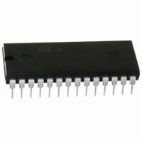
M5480B7 STMicroelectronics, M5480B7 Datasheet - Page 3

M5480B7
Manufacturer Part Number
M5480B7
Description
IC LED DISPLAY DRIVER 28-PDIP
Manufacturer
STMicroelectronics
Datasheet
1.M5480B7.pdf
(10 pages)
Specifications of M5480B7
Display Type
LED
Configuration
7 Segment
Interface
Serial
Digits Or Characters
3.5 Digits
Current - Supply
7mA
Voltage - Supply
4.75 V ~ 13.2 V
Operating Temperature
-25°C ~ 85°C
Mounting Type
Through Hole
Package / Case
28-DIP (0.600", 15.24mm)
Number Of Digits
3.5
Number Of Segments
23
Operating Supply Voltage
13.2 V
Maximum Supply Current
7 mA
Maximum Power Dissipation
940 mW
Maximum Operating Temperature
+ 85 C
Mounting Style
Through Hole
Minimum Operating Temperature
- 25 C
Lead Free Status / RoHS Status
Lead free / RoHS Compliant
Available stocks
Company
Part Number
Manufacturer
Quantity
Price
Company:
Part Number:
M5480B7
Manufacturer:
XICOR
Quantity:
6 217
Table 1. Absolute Maximum Ratings
Note: Stresses in excess of those listed under "Absolute Maximum Ratings" may cause permanent damage to the device. This is a stress
Table 2. Static Electrical Characteristics
Note: 1. Output matching is calculated as the percent variation from I
(T
Symbol
amb
V
f
V
clock
I
O(off)
V
DD
V
I
I
rating only and functional operation of the device at these or any other conditions in excess of those indicated in the operational sec-
tions of this specification is not implied. Exposure to absolute maximum rating conditions for extended periods may affect device reli-
ability.
I
Symbol
2. With a fixed resistor on the brightness input some variation in brightness will occur from one device to another.
3. Absolute maximum for each output should be limited to 40mA.
4. The VO voltage should be regulated by the user.
DD
O
O
B
B
V
I
P
T
V
T
within operating range, V
O(off)
STG
V
I
TOT
T
OP
DD
O
I
j
Supply Voltage.,75
Supply Current
Input Voltage Logical "0" Level
Logical "1" Level
Brightness Input Current (note 2)
Brightness Input Voltage (pin 13)
Off State Out. Voltage
Out. Sink Current (note 3)
Segment OFF
Segment ON
Input Clock Frequency
Output Matching (note 1)
Supply Voltage
Input Voltage
Off State Output Voltage
Output Sink Current
Total Package Power Dissipation at 25°C
Junction Temperature
Operating Temperature Range
Storage Temperature Range
Total Package Power Dissipation at 85°C
Parameter
DD
= 4.75V to 13.2V, V
Parameter
V
± 10µA Input Bias
4.75 ≤ V
V
Input Current = 750µA, T
V
V
Brightness In. = 0µA
Brightness In. = 100µA
Brightness In. = 750µA
O
O
DD
DD
= 3V
= 1V (note 4)
= 13.2V
> 5.25
DD
Test Conditions
MAX
≤ 5.25
SS
+ I
= 0V, unless otherwise specified)
MIN
/2.
amb
= 25°C
V
- 0.3
Min.
2.2
DD
12
0
3
0
2
0
– 65 to 150
– 0.3 to 15
– 0.3 to 15
– 25 to 85
- 2
Value
940
490
150
15
40
Typ.
13.2
2,7
15
Max.
13.2
0.08
0.75
4.3
± 20
V
V
0.5
18
10
10
25
7
4
DD
DD
M5480
Unit
mW
mW
mA
°C
°C
°C
V
V
V
MHz
Unit
V
mA
mA
mA
µA
µA
mA
%
3/10
V
V
V
V
V


