STLVDS385BTR STMicroelectronics, STLVDS385BTR Datasheet
STLVDS385BTR
Specifications of STLVDS385BTR
Available stocks


Related parts for STLVDS385BTR


STLVDS385BTR Summary of contents
Page 1
... A rising Table 1. Device summary Order code Temperature range STLVDS385BTR - °C January 2009 + 3.3 V programmable LVDS transmitter 24-bit flat panel display (FPD) link-85 MHz edge or falling edge strobe transmitter will inter operate with a falling edge strobe receiver without any translation logic ...
Page 2
Contents 1 Pin configuration . . . . . . . . . . . . . . . . . . . . . . . . . . . . . . . . . . . . ...
Page 3
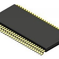
Pin configuration Figure 1. Pin configuration 3/19 ...
Page 4
Table 2. Pin description Pin n° Symbol 10, 11, 12, 14, 15, 16, 18, 19, 20, 22, T 23, 24, 25, 27, 28, 30, 50, 51, 52, 54, 55, 56 ...
Page 5
Maximum ratings Table 4. Absolute maximum ratings Symbol V Supply voltage CC V CMOS/TTL input voltage I V LVDS driver output voltage DO I LVDS output short circuit duration OSD HBM ESD EIAJ I Latch up tolerance LATCH T ...
Page 6
Electrical characteristics Table 7. LVCMOS/LVTTL DC specifications (V Typical values are referred to T Symbol Parameter V High level input voltage IH V Low level input voltage IL V Input clamp voltage CL I Input current I Table 8. ...
Page 7
Table 10. Transmitter switching characteristics (V noted. Typical values are referred to T Symbol Parameter LVDS low-to-high transition time t LLHT (Figure 5) LVDS high-to-low transition time t LLLT (Figure 5) Transmitter output pulse position for bit 0 t TPP0 ...
Page 8
Table 10. Transmitter switching characteristics (continued) (V otherwise noted. Typical values are referred to T Symbol Parameter t Transmitter phase lock loop set PLLS t Transmitter power down delay PDD Note: 1 Current into device pins is defined as positive. ...
Page 9
AC timing diagrams Figure 2. Worst case test pattern 1. The worst case test pattern produces a maximum toggling of digital circuits, LVDS I/O and CMOS/TTL I/O. (1) 9/19 ...
Page 10
Figure 3. 16 grayscale test patter 1. The 16 grayscale test pattern tests device power consumption for a “typical” LCD display pattern. The test pattern approximates signal switching needed to produce groups of 16 vertical stripes across the display. 2. ...
Page 11
Figure 4. (Transmitter) LVDS output load Figure 5. (Transmitter) LVDS transition time Figure 6. (Transmitter) input clock transition time 11/19 ...
Page 12
Figure 7. (Transmitter) setup/hold and high/low times (falling edge strobe) Figure 8. (Transmitter) clock in to clock out delay 12/19 ...
Page 13
Figure 9. (Transmitter) phase lock loop set time Figure 10. 28 parallel TTL data inputs mapped to LVDS outputs 13/19 ...
Page 14
Figure 11. Transmitter power down delay Figure 12. Transmitter LVDS output pulse position measurement 14/19 ...
Page 15
Package mechanical data In order to meet environmental requirements, ST offers these devices in different grades of ECOPACK® packages, depending on their level of environmental compliance. ECOPACK® specifications, grade definitions and product status are available at: ECOPACK® ...
Page 16
Dim. Min 0. 0.17 c 0.09 D 13.9 E 7. 0° PIN 1 IDENTIFICATION 1 16/19 TSSOP56 mechanical data mm. Typ. Max. 1.2 0.15 0.002 0.9 ...
Page 17
Tape and reel TSSOP56 mechanical data mm. Dim. Min. Typ 12 8.7 Bo 17.2 Ko 1.4 Po 3.9 P 11.9 inch. Max. Min. Typ. 330 13.2 0.504 0.795 2.362 30.4 8.9 0.342 ...
Page 18
Revision history Table 11. Document revision history Date Revision 21-Jun-2004 1 26-Jan-2009 2 18/19 Changes First release. Modified Table 1 on page 1. ...
Page 19
... Information in this document is provided solely in connection with ST products. STMicroelectronics NV and its subsidiaries (“ST”) reserve the right to make changes, corrections, modifications or improvements, to this document, and the products and services described herein at any time, without notice. All ST products are sold pursuant to ST’s terms and conditions of sale. ...