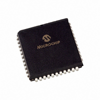
TC820CLW713 Microchip Technology, TC820CLW713 Datasheet - Page 20

TC820CLW713
Manufacturer Part Number
TC820CLW713
Description
IC ADC 3 3/4DGT LGC PROBE 44PLCC
Manufacturer
Microchip Technology
Datasheet
1.TC820CPL.pdf
(34 pages)
Specifications of TC820CLW713
Display Type
LCD
Configuration
7 Segment + 2 Annunciators
Digits Or Characters
A/D 3.75 Digits
Current - Supply
1mA
Voltage - Supply
9V
Operating Temperature
0°C ~ 70°C
Mounting Type
Surface Mount
Package / Case
44-PLCC
Lead Free Status / RoHS Status
Request inventory verification / Request inventory verification
Interface
-
Available stocks
Company
Part Number
Manufacturer
Quantity
Price
Company:
Part Number:
TC820CLW713
Manufacturer:
Microchip Technology
Quantity:
10 000
TC820
5.8
The TC820 true differential input and differential
reference make ratiometric readings possible. In ratio-
metric operation, an unknown resistance is measured
with respect to a known standard resistance. No
accurately defined reference voltage is needed.
The unknown resistance is put in series with a known
standard and a current is passed through the pair
(Figure
is applied to the input and voltages across the known
resistor applied to the reference input. If the unknown
equals the standard, the input voltage will equal the refer-
ence voltage and the display will read 2000. The displayed
reading can be determined from the following expression:
EQUATION 5-3:
The display will over range for values of R
≥ 2 x R
FIGURE 5-8:
Ratiometric Resistance Measurement.
5.9
When the FREQ/VOLTS input is high and the LOGIC
input is low, the TC820 will count pulses at the RANGE/
FREQ input. The time-base will be F
1 second with a 40kHz clock. The signal to be
measured should swing from V
RANGE/FREQ input has CMOS input levels without
hysteresis. For best results, especially with low
frequency sine-wave inputs, an external buffer with
hysteresis should be added. A typical circuit is shown
in
DS21476C-page 20
R
Figure
UNKNOWN
R
STANDARD
STANDARD
5-8). The voltage developed across the unknown
Displayed Reading =
Ratiometric Resistance
Measurements
Buffering the FREQ Input
5-9.
.
V
V
V
V
Analog
Common
Low Parts Count
REF
REF
IN
IN
TC820
+
-
V
+
-
DD
R
R
STANDARD
UNKNOWN
DD
to DGND. The
OSC
LCD
/40,000, or
UNKNOWN
FIGURE 5-9:
Buffer.
5.10
The DP0/LO and DP1/HI inputs provide the logic probe
inputs when the LOGIC input is high. Driving either
DP0/LO or DP1/HI to a logic high will turn on the
appropriate LCD annunciator. When DP0/LO is high,
the buzzer will be on.
To provide a "single input" logic probe function, external
buffers should be used. A simple circuit is shown in
Figure
ciator on for high and low level inputs.
FIGURE 5-10:
Buffer.
If carefully controlled logic thresholds are required, a
window comparator can be used.
typical circuit. This circuit will turn on the high or low
annunciators when the logic thresholds are exceeded,
but the resistors connected from DP0/LO and DP1/HI
to DGND will turn both annunciators off when the logic
probe is unconnected.
The TC820 logic inputs are not latched internally, so
pulses of short duration will usually be difficult or
impossible to see. To display short pulses properly, the
input pulse should be "stretched." The circuit of
Figure 5-11
pull-down resistors to stretch the input pulse and permit
viewing short duration input pulses.
Frequency
Logic
Probe
Input
Input
GND
5-10. This circuit will turn the appropriate annun-
Logic Probe Inputs
DGND
shows capacitors added across the input
+
1µF
*
Frequency Counter External
Simple External Logic Probe
74HC14
+9V
*74HC14
© 2007 Microchip Technology Inc.
TC820
*
+9V
Figure 5-11
FREQ/VOLTS
RANGE/FREQ
DGND
V
DD
V
LOGIC
DP1/HI
DP0/LO
DGND
DD
TC820
shows a


