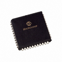
TC820CLW713 Microchip Technology, TC820CLW713 Datasheet - Page 17

TC820CLW713
Manufacturer Part Number
TC820CLW713
Description
IC ADC 3 3/4DGT LGC PROBE 44PLCC
Manufacturer
Microchip Technology
Datasheet
1.TC820CPL.pdf
(34 pages)
Specifications of TC820CLW713
Display Type
LCD
Configuration
7 Segment + 2 Annunciators
Digits Or Characters
A/D 3.75 Digits
Current - Supply
1mA
Voltage - Supply
9V
Operating Temperature
0°C ~ 70°C
Mounting Type
Surface Mount
Package / Case
44-PLCC
Lead Free Status / RoHS Status
Request inventory verification / Request inventory verification
Interface
-
Available stocks
Company
Part Number
Manufacturer
Quantity
Price
Company:
Part Number:
TC820CLW713
Manufacturer:
Microchip Technology
Quantity:
10 000
5.0
5.1
The TC820 is designed to operate from a single power
supply such as a 9V battery
will operate over a range of 7V to 15V. For battery oper-
ation, analog common (COM) provides a Common
mode bias voltage (see analog common discussion in
the theory of operation section). However, measure-
ments cannot be referenced to battery ground. To do so
will exceed the Negative Common mode voltage limit.
FIGURE 5-1:
Single 9V Battery.
A battery with voltage between 3.5V and 7V can be
used to power the TC820, when used with a voltage
doubler, as shown in
uses the TC7660 and two external capacitors. With this
configuration, measurements can be referenced either
to analog common or to battery ground.
FIGURE 5-2:
Low Voltage Battery.
© 2007 Microchip Technology Inc.
+
–
+
3.5V to 6V
+
10µF
9V
2
4
TYPICAL APPLICATIONS
Power Supplies
TC7660
TC820
8
3
V
V
DD
SS
V
V
10µF
5
+
REF
COM
REF
V
V
Figure
Powering the
Powering the
IN
IN
+
+
-
-
TC820
V
V
(Figure
DD
SS
5-2. The voltage doubler
V
V
REF
REF
COM
V
V
IN
IN
+
+
5-1). The converter
-
-
TC820
TC820
from a
from a
V
V
IN
IN
+
+
–
–
5.2
Digital ground is generated from an internal zener
diode
DGND is the internal supply voltage for the digital
section of the TC820. DGND will sink a minimum of
3 mA.
DGND establishes the low logic level reference for the
TC820 mode select inputs, and for the frequency and
logic probe inputs. The DGND pin can be used as the
negative supply for external logic gates, such as the
logic probe buffers. To ensure correct counter
operation at high frequency, connect a 1 µF capacitor
from DGND to V
DGND also provides the drive voltage for the LCD. The
TC820 40-pin package internally connects the LCD
V
of about 5V
V
FIGURE 5-3:
5.3
Logic levels for the TC820 digital inputs are referenced
to V
V
most cases, digital inputs will be connected directly to
V
be used to control the logic inputs, as shown in the logic
probe inputs section.
5.4
The TC820 oscillator can be controlled with either a
crystal, or with an inexpensive resistor capacitor
combination. The crystal circuit, shown in
recommended when high accuracy is required in the
Frequency Counter mode. The 40 kHz crystal is a stan-
dard frequency for ultrasonic alarms, and will provide a
1-second time-base for the counter or 2.5 analog-to-
digital conversions per second. Consult the crystal
manufacturer for detailed applications information.
DISP
DISP
DD
DD
– 1.5V, and the low logic level is DGND + 1.5V. In
with a mechanical switch. CMOS gates can also
DD
pin to DGND, and provides an LCD drive voltage
pin to DGND will provide a 5V LCD drive voltage.
(Figure
TC820
Digital Ground (DGND)
Digital Input Logic Levels
Clock Oscillator
and DGND. The high level threshold is
–
+
P-P
12µA
. In the 44-pin package, connecting the
5-3). The voltage between V
DD
N
.
DGND and Com Outputs.
N
Section
Logic
P
DS21476C-page 17
TC820
5V
Figure
3.2V
DD
V
COM
DGND
V
5-4, is
DD
SS
and


