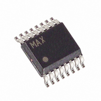
MAX6852AEE+ Maxim Integrated Products, MAX6852AEE+ Datasheet - Page 13

MAX6852AEE+
Manufacturer Part Number
MAX6852AEE+
Description
IC VFD CTRLR MATRIX 16QSOP
Manufacturer
Maxim Integrated Products
Datasheet
1.MAX6852AEET.pdf
(32 pages)
Specifications of MAX6852AEE+
Display Type
Vacuum Fluorescent (VF)
Configuration
5 x 7 (Matrix)
Interface
Serial
Current - Supply
3.5mA
Voltage - Supply
2.7 V ~ 3.6 V
Operating Temperature
-40°C ~ 125°C
Mounting Type
Surface Mount
Package / Case
16-QSOP
Lead Free Status / RoHS Status
Lead free / RoHS Compliant
Digits Or Characters
-
Controlling the MAX6852 requires sending a 16-bit
word. The first byte, D15 through D8, is the command
address, and the second byte, D7 through D0, is the
data to be written to the command address (Table 23).
Daisy-chain multiple MAX6852s by connecting the
DOUT of one device to the DIN of the next, and driving
SCLK and CS lines in parallel. Data at DIN propagates
through the internal shift registers and appears at
DOUT 15.5 clock cycles later, clocked out on the rising
edge of SCLK. When sending commands to daisy-
chained MAX6852s, all devices are accessed at the
same time. An access requires (16 x n) clock cycles,
where n is the number of MAX6852s connected togeth-
er. To update just one device in a daisy-chain, send the
no-op command (0x00) to the others. Care must be
taken on power-up when daisy-chaining the serial inter-
face in this manner. Configure each MAX6852’s PORT0
or PORT1 outputs, in turn, to act as DOUT before data
propagates through it. For this reason, PORT0 is the
preferred output to configure as DOUT because its out-
put on power-up is low. This means that a daisy-
chained DIN input taking data from an uninitialized
PORT0 output clocks in 16 logic zeros, which is the
safe no-op instruction.
The MAX6852 contains a 16-bit shift register into which
DIN is clocked on the rising edge of SCLK, when CS is
low. When CS is high, transitions on SCLK have no
effect. When CS goes high, the 16 bits in the shift regis-
ter are parallel loaded into a 16-bit latch. The 16 bits in
the latch are then decoded and executed.
The MAX6852 is written to using the following
sequence:
1) Take SCLK low.
2) Take CS low. This enables the internal 16-bit shift
3) Clock 16 bits of data into DIN, D15 first to D0 last,
4) Take CS high (while SCLK is still high after clocking
5) Take SCLK low.
Figure 7 shows a write operation when 16 bits are
transmitted.
register.
observing the setup and hold times. Bit D15 is low,
indicating a write command.
in the last data bit).
Control and Operation Using the 4-Wire
Connecting Multiple MAX6852s to the
______________________________________________________________________________________
4-Wire Interfaced, 5
Writing Device Registers
4-Wire Bus
Fluorescent Display Controller
Interface
Table 7. Character Map
LSB
1010
0000
0001
0011
0100
1000
1100
1101
1110
1111
0010
0101
0110
0111
1001
1011
MSB
RAM06
RAM07
RAM00
RAM01
RAM02
RAM04
RAM05
RAM08
RAM09
RAM10
RAM11
RAM12
RAM13
RAM14
RAM15
RAM03
x000
✕
7 Matrix Vacuum-
RAM16
RAM19
RAM21
RAM22
RAM23
RAM17
RAM18
RAM20
x001
x010
x011
x100
x101
x110
x111
13


