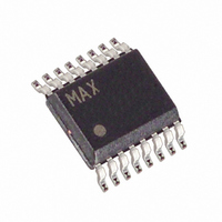
MAX6852AEE+T Maxim Integrated Products, MAX6852AEE+T Datasheet - Page 14

MAX6852AEE+T
Manufacturer Part Number
MAX6852AEE+T
Description
IC VFD CTRLR MATRIX 16QSOP
Manufacturer
Maxim Integrated Products
Datasheet
1.MAX6852AEET.pdf
(32 pages)
Specifications of MAX6852AEE+T
Display Type
Vacuum Fluorescent (VF)
Configuration
5 x 7 (Matrix)
Interface
Serial
Current - Supply
3.5mA
Voltage - Supply
2.7 V ~ 3.6 V
Operating Temperature
-40°C ~ 125°C
Mounting Type
Surface Mount
Package / Case
16-QSOP
Lead Free Status / RoHS Status
Lead free / RoHS Compliant
Digits Or Characters
-
4-Wire Interfaced, 5
Fluorescent Display Controller
Figure 6. 4-Wire Serial Interface Timing Diagram
Figure 7. 16-Bit Write Transmission to the MAX6852
If fewer or greater than 16 bits are clocked into the
MAX6852 between taking CS low and taking CS high
again, the MAX6852 stores the last 16 bits received,
including the previous transmission(s). The general
case is when n bits (where n > 16) are transmitted to
the MAX6852. The last bits comprising bits {n-15} to {n}
are retained and are parallel loaded into the 16-bit latch
as bits D15 to D0, respectively (Figure 8).
Any register data within the MAX6852 may be read by
sending a logic high to bit D15. The sequence is:
1) Take SCLK low.
2) Take CS low. This enables the internal 16-bit shift
3) Clock 16 bits of data into DIN, D15 first to D0 last,
14
DOUT
CLK
DIN
CS
register.
observing the setup and hold times. Bit D15 is high,
indicating a read command, and bits D14 through
______________________________________________________________________________________
SCLK
DOUT
DIN
CS
D15
= 0
D14
Reading Device Registers
D13
D12
t
CSS
D11
t
DS
DN
t
DH
D10
t
CL
D9
✕
DN-1
t
CH
7 Matrix Vacuum-
D8
4) Take CS high. Positions D7 through D0 in the shift
5) Take SCLK low.
6) Issue another read or write command (which can be
The VFD driver interface on the MAX6852 is a serial
interface using three output pins, VFLOAD, VFCLK, and
VFDOUT (Figure 9) to drive industry-standard, shift-reg-
D7
D8 contain the address of the register to read. Bits
D7 to D0 contain dummy data, which is discarded.
register are now loaded with the data in the register
addressed by bits D15 through D8.
no-op), and examine the bit stream at DOUT; the
first 8 bits contain the address of the register that
was read (Note: The MSB, which was transmitted as
a 1 for a read command, may read back either as a
1 or a zero). The second 8 bits are the contents of
the register addressed by bits D14 through D8 in
Step 3.
D1
D6
t
CP
D5
D0
t
CSH
D4
VFD Driver Serial Interface
D3
t
CSW
D15
t
CSU
D2
D1
D0
D15 = 0


