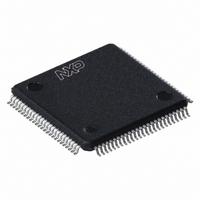
PCF2113DH/4,557 NXP Semiconductors, PCF2113DH/4,557 Datasheet - Page 33

PCF2113DH/4,557
Manufacturer Part Number
PCF2113DH/4,557
Description
IC LCD CONTROLLER/DRIVER 100LQFP
Manufacturer
NXP Semiconductors
Datasheet
1.PCF2113DH4557.pdf
(65 pages)
Specifications of PCF2113DH/4,557
Package / Case
100-LQFP
Display Type
LCD
Configuration
5 X 8 (Matrix)
Interface
I²C
Voltage - Supply
2.2 V ~ 4 V
Operating Temperature
-40°C ~ 85°C
Mounting Type
Surface Mount
Number Of Digits
40
Maximum Clock Frequency
450 KHz
Operating Supply Voltage
1.8 V to 5.5 V
Maximum Power Dissipation
400 mW
Maximum Operating Temperature
+ 75 C
Attached Touch Screen
No
Maximum Supply Current
50 mA
Minimum Operating Temperature
- 20 C
Operating Supply Voltage (typ)
2.5/3.3/5V
Package Type
LQFP
Pin Count
100
Mounting
Surface Mount
Power Dissipation
400mW
Operating Supply Voltage (min)
1.8V
Operating Supply Voltage (max)
5.5V
Lead Free Status / RoHS Status
Lead free / RoHS Compliant
Current - Supply
-
Digits Or Characters
-
Lead Free Status / Rohs Status
Lead free / RoHS Compliant
Other names
935276328557
PCF2113DH/4
PCF2113DH/4
PCF2113DH/4
PCF2113DH/4
Available stocks
Company
Part Number
Manufacturer
Quantity
Price
Company:
Part Number:
PCF2113DH/4,557
Manufacturer:
NXP Semiconductors
Quantity:
10 000
NXP Semiconductors
PCF2113_FAM_4
Product data sheet
10.6.1 Bits S1 and S0
10.7.1 Bit L
10.5 Direct mode
10.6 Voltage multiplier control
10.7 Screen configuration
Icon states for the even phase are stored in CGRAM characters 0 to 2
(3
used (see
Icon states for the odd phase are stored in CGRAM characters 4 to 6 (another 120 bits for
the 120 icons). When icon blink is disabled CGRAM characters 4 to 6 may be used as
normal CGRAM characters.
Table 13.
When DM = 0, the chip is not in the Direct mode. Either the internal V
external voltage may be used to achieve V
When DM = 1, the chip is in Direct mode. The internal V
output V
The Direct mode can be used to reduce the current consumption when the required
output voltage V
mode or in MUX 1:9 (depending on LCD liquid properties).
A software configurable voltage multiplier is incorporated in the V
be set via the ‘Set HVgen stages’ command.
The voltage multiplier control can be used to reduce current consumption by
disconnecting internal voltage multiplier stages, depending on the required output voltage
V
Table 14.
L = 0: the two halves of a split screen are connected in a standard way i.e. column 1/61,
2/62 to 60/120; default.
L = 1: the two halves of a split screen are connected in a mirrored way i.e. column 1/120,
2/119 to 60/61. This allows single layer PCB or glass layout.
Parameter
Cursor character blink
Icons
S1
0
0
1
1
LCD
8
(see
5 = 120 bits for 120 icons). These bits also define icon state when icon blink is not
LCDOUT
Table
Table
Blink effect for icons and cursor character blink
S1 and S0 control of voltage multiplier
is directly connected V
LCDOUT
13).
14).
S0
0
1
0
1
Rev. 04 — 4 March 2008
is close to the V
Even phase
block (all on)
state 1; CGRAM character 0 to 2
Description
set V
set V
set V
do not use
DD2
DD2
LCD
LCD
LCD
LCD
(i.e. the V
supply voltage. This can be the case in Icon
generator stages to 1 (2
generator stages to 2 (3
generator stages to 3 (4
.
LCD
LCD
generator supply voltage).
Odd phase
normal (display character)
state 2; CGRAM character 4 to 6
generator is turned off and the
LCD controllers/drivers
LCD
PCF2113x
voltage multiplier)
voltage multiplier)
voltage multiplier)
generator and can
LCD
© NXP B.V. 2008. All rights reserved.
generator or an
33 of 65


