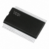
PCF8576T/1,118 NXP Semiconductors, PCF8576T/1,118 Datasheet - Page 24

PCF8576T/1,118
Manufacturer Part Number
PCF8576T/1,118
Description
IC LCD DRV UNVRSL LOW-MUX 56VSOP
Manufacturer
NXP Semiconductors
Datasheet
1.PCF8576T1118.pdf
(44 pages)
Specifications of PCF8576T/1,118
Package / Case
56-VSOP
Display Type
LCD
Configuration
40 Segment
Interface
I²C
Current - Supply
180µA
Voltage - Supply
2 V ~ 9 V
Operating Temperature
-40°C ~ 85°C
Mounting Type
Surface Mount
Number Of Digits
20
Number Of Segments
160
Maximum Clock Frequency
288 KHz
Operating Supply Voltage
2 V to 9 V
Maximum Power Dissipation
400 mW
Maximum Supply Current
180 uA
Lead Free Status / RoHS Status
Lead free / RoHS Compliant
Digits Or Characters
-
Lead Free Status / Rohs Status
Lead free / RoHS Compliant
Other names
933804620118
PCF8576T/1-T
PCF8576T/1-T
PCF8576T/1-T
PCF8576T/1-T
Philips Semiconductors
Table 12 BANK SELECT option 2
Table 13 BLINK option 1
Table 14 BLINK option 2
7.9
The display controller executes the commands identified
by the command decoder. It contains the status registers
of the PCF8576 and co-ordinates their effects. The
controller is also responsible for loading display data into
the display RAM as required by the filling order.
2001 Oct 02
RAM bit 0
RAM bit 2
Off
2 Hz
1 Hz
0.5 Hz
Normal blinking
Alternation blinking
Universal LCD driver for low multiplex rates
BLINK FREQUENCY
STATIC
Display controller
BLINK MODE
RAM bits 0 and 1
RAM bits 2 and 3
1 : 2 MUX
BF1
0
0
1
1
BIT A
BITS
0
1
BIT O
0
1
BF0
0
1
0
1
24
7.10
In large display configurations, up to 16 PCF8576s can be
distinguished on the same I
hardware subaddress (A0, A1 and A2) and the
programmable I
cascaded PCF8576s are synchronized so that they can
share the backplane signals from one of the devices in the
cascade. Such an arrangement is cost-effective in large
LCD applications since the backplane outputs of only one
device need to be through-plated to the backplane
electrodes of the display. The other PCF8576s of the
cascade contribute additional segment outputs but their
backplane outputs are left open-circuit (see Fig.18).
The SYNC line is provided to maintain the correct
synchronization between all cascaded PCF8576s. This
synchronization is guaranteed after the Power-on reset.
The only time that SYNC is likely to be needed is if
synchronization is accidentally lost (e.g. by noise in
adverse electrical environments; or by the definition of a
multiplex mode when PCF8576s with differing SA0 levels
are cascaded). SYNC is organized as an input/output pin;
the output selection being realized as an open-drain driver
with an internal pull-up resistor. A PCF8576 asserts the
SYNC line at the onset of its last active backplane signal
and monitors the SYNC line at all other times. Should
synchronization in the cascade be lost, it will be restored
by the first PCF8576 to assert SYNC. The timing
relationship between the backplane waveforms and the
SYNC signal for the various drive modes of the PCF8576
are shown in Fig.19.
For single plane wiring of packaged PCF8576s and
chip-on-glass cascading, see Chapter 12.
Cascaded operation
2
C-bus slave address (SA0). When
2
C-bus by using the 3-bit
Product specification
PCF8576


