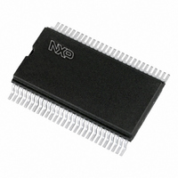
PCF8576CT/1,112 NXP Semiconductors, PCF8576CT/1,112 Datasheet - Page 10

PCF8576CT/1,112
Manufacturer Part Number
PCF8576CT/1,112
Description
IC LCD DVR UNVRSL LOW-MUX 56VSOP
Manufacturer
NXP Semiconductors
Specifications of PCF8576CT/1,112
Package / Case
56-VSOP
Display Type
LCD
Configuration
40 Segment
Interface
I²C
Current - Supply
120µA
Voltage - Supply
2 V ~ 6 V
Operating Temperature
-40°C ~ 85°C
Mounting Type
Surface Mount
Number Of Digits
20
Number Of Segments
160
Maximum Clock Frequency
315 KHz
Operating Supply Voltage
2 V to 6 V
Maximum Power Dissipation
400 mW
Maximum Operating Temperature
+ 85 C
Attached Touch Screen
No
Maximum Supply Current
120 uA
Minimum Operating Temperature
- 40 C
Lead Free Status / RoHS Status
Lead free / RoHS Compliant
Digits Or Characters
-
Lead Free Status / Rohs Status
Lead free / RoHS Compliant
Other names
935278818112
PCF8576CTD
PCF8576CTD
PCF8576CTD
PCF8576CTD
NXP Semiconductors
PCF8576C
Product data sheet
7.1 Power-On-Reset (POR)
7.2 LCD bias generator
The host microprocessor or microcontroller maintains the 2-line I
channel with the PCF8576C.
Biasing voltages for the multiplexed LCD waveforms are generated internally, removing
the need for an external bias generator. The internal oscillator is selected by connecting
pin OSC to V
power supplies (pins V
At power-on the PCF8576C resets to the following starting conditions:
Remark: Do not transfer data on the I
the reset action to complete.
The full-scale LCD voltage (V
temperature compensated externally through the V
Fractional LCD biasing voltages are obtained from an internal voltage divider comprising
three series resistors connected between V
switched out of the circuit to provide a
configuration.
Fig 7.
•
•
•
•
•
•
All backplane and segment outputs are set to V
The selected drive mode is 1:4 multiplex with
Blinking is switched off
Input and output bank selectors are reset (as defined in
The I
The data pointer and the subaddress counter are cleared
V
V
DD
SS
CONTROLLER
2
PROCESSOR/
Typical system configuration
C-bus interface is initialized
MICRO-
MICRO-
HOST
SS
. The only other connections required to complete the system are the
All information provided in this document is subject to legal disclaimers.
R≤
2C
t
r
B
DD
Rev. 10 — 22 July 2010
, V
SS
oper
, and V
OSC
SDA
SCL
) is obtained from V
LCD
2
A0
1
C-bus for at least 1 ms after a power-on to allow
⁄
2
V
PCF8576C
) and the LCD panel selected for the application.
DD
bias voltage level for the 1:2 multiplex
A1
Universal LCD driver for low multiplex rates
DD
A2
and V
V
LCD
SA0 V
1
⁄
LCD
3
DD
DD
LCD
bias
SS
supply to pin V
40 segment drives
− V
. The center resistor can be
4 backplanes
LCD
Table
. The LCD voltage may be
2
C-bus communication
8)
PCF8576C
LCD
© NXP B.V. 2010. All rights reserved.
LCD PANEL
(up to 160
elements)
.
013aaa098
10 of 57


