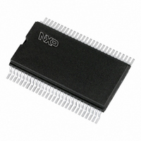
PCF8576CT/1,112 NXP Semiconductors, PCF8576CT/1,112 Datasheet - Page 23

PCF8576CT/1,112
Manufacturer Part Number
PCF8576CT/1,112
Description
IC LCD DVR UNVRSL LOW-MUX 56VSOP
Manufacturer
NXP Semiconductors
Specifications of PCF8576CT/1,112
Package / Case
56-VSOP
Display Type
LCD
Configuration
40 Segment
Interface
I²C
Current - Supply
120µA
Voltage - Supply
2 V ~ 6 V
Operating Temperature
-40°C ~ 85°C
Mounting Type
Surface Mount
Number Of Digits
20
Number Of Segments
160
Maximum Clock Frequency
315 KHz
Operating Supply Voltage
2 V to 6 V
Maximum Power Dissipation
400 mW
Maximum Operating Temperature
+ 85 C
Attached Touch Screen
No
Maximum Supply Current
120 uA
Minimum Operating Temperature
- 40 C
Lead Free Status / RoHS Status
Lead free / RoHS Compliant
Digits Or Characters
-
Lead Free Status / Rohs Status
Lead free / RoHS Compliant
Other names
935278818112
PCF8576CTD
PCF8576CTD
PCF8576CTD
PCF8576CTD
Philips Semiconductors
Table 4 Definition of PCF8576 commands
Table 5 MODE SET option 1
Table 6 MODE SET option 2
Table 7 MODE SET option 3
2001 Oct 02
MODE SET C 1
LOAD DATA
POINTER
DEVICE
SELECT
BANK
SELECT
BLINK
Static
1 : 2
1 : 3
1 : 4
1
1
Disabled (blank)
Enabled
COMMAND
DRIVE MODE
3
2
Universal LCD driver for low multiplex rates
bias
bias
DISPLAY STATUS
LCD DRIVE MODE
LCD BIAS
C 0 P5 P4 P3 P2
C 1
C 1
C 1
1 BP
MUX (2 BP)
MUX (3 BP)
MUX (4 BP)
BACKPLANE
0
1
1
1
LP
0
1
1
OPCODE
E
0
1
0
A2
B
A
0
BF1 BF0
BIT B
M1
M1
BIT E
P1
A1
0
1
1
0
I
0
1
0
1
BITS
M0
P0
A0
O
M0
OPTIONS
1
0
1
0
Table 10
Table 11
Table 12
Table 13
Table 14
Table 5
Table 6
Table 7
Table 8
Table 9
23
Table 8 MODE SET option 4
Table 9 LOAD DATA POINTER option 1
Table 10 DEVICE SELECT option 1
Table 11 BANK SELECT option 1
Normal mode
Power-saving mode
6-bit binary value of 0 to 39 P5 P4 P3 P2 P1 P0
3-bit binary value of 0 to 7
RAM bit 0
RAM bit 2
Defines LCD drive mode.
Defines LCD bias configuration.
Defines display status. The possibility to disable the
display allows implementation of blinking under
external control.
Defines power dissipation mode.
Six bits of immediate data, bits P5 to P0, are
transferred to the data pointer to define one of forty
display RAM addresses.
Three bits of immediate data, bits A2 to A0, are
transferred to the subaddress counter to define one of
eight hardware subaddresses.
Defines input bank selection (storage of arriving
display data).
Defines output bank selection (retrieval of LCD display
data). The BANK SELECT command has no effect in
1 : 3 and 1 : 4 multiplex drive modes.
Defines the blinking frequency.
Selects the blinking mode; normal operation with
frequency set by BF1, BF0 or blinking by alternation of
display RAM banks. Alternation blinking does not
apply in 1 : 3 and 1 : 4 multiplex drive modes.
STATIC
DESCRIPTION
DESCRIPTION
MODE
RAM bits 0 and 1
RAM bits 2 and 3
DESCRIPTION
1 : 2 MUX
A2
Product specification
BIT LP
BITS
BITS
PCF8576
A1
0
1
BIT I
0
1
A0


