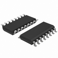
74HCT4511D,652 NXP Semiconductors, 74HCT4511D,652 Datasheet - Page 10

74HCT4511D,652
Manufacturer Part Number
74HCT4511D,652
Description
IC BCD-7SEG LATCH/DEC/DVR 16SOIC
Manufacturer
NXP Semiconductors
Datasheets
1.74HCT4046ADB112.pdf
(19 pages)
2.74HCT4046ADB112.pdf
(23 pages)
3.74HC4511D653.pdf
(12 pages)
Specifications of 74HCT4511D,652
Package / Case
16-SOIC (3.9mm Width)
Display Type
LED
Configuration
7 Segment
Interface
BCD
Voltage - Supply
4.5 V ~ 5.5 V
Operating Temperature
-40°C ~ 125°C
Mounting Type
Surface Mount
Product
Latch/Decoder/Driver
Logic Family
74HCT
Number Of Lines (input / Output)
7.0 / 7.0
Propagation Delay Time
13 ns
Supply Voltage (max)
5.5 V
Supply Voltage (min)
4.5 V
Maximum Operating Temperature
+ 125 C
Minimum Operating Temperature
- 40 C
Mounting Style
SMD/SMT
Number Of Input Lines
7.0
Number Of Output Lines
7.0
Lead Free Status / RoHS Status
Lead free / RoHS Compliant
Current - Supply
-
Digits Or Characters
-
Lead Free Status / Rohs Status
Lead free / RoHS Compliant
Other names
568-2875-5
933715360652
933715360652
Philips Semiconductors
AC WAVEFORMS
December 1990
BCD to 7-segment latch/decoder/driver
(1) HC : V
Fig.8
(1) HC : V
Fig.10 Waveforms showing the input (BI) to output
HCT: V
HCT: V
Waveforms showing the input (D
output (Q
output transition times.
(Q
M
M
M
M
n
= 50%; V
= 50%; V
= 1.3 V; V
= 1.3 V; V
) propagation delays.
n
I
I
I
) propagation delays and the
I
= GND to V
= GND to V
= GND to 3 V.
= GND to 3 V.
CC
CC
.
.
n
, LT) to
10
(1) HC : V
Fig.9
The shaded areas indicate when the input is
permitted to change for predictable output
performance.
(1) HC : V
Fig.11 Waveforms showing the data set-up and
HCT: V
HCT: V
Waveforms showing the input (LE) to output
(Q
enable pulse width.
hold times for D
M
M
M
M
n
= 50%; V
= 1.3 V; V
= 50%; V
= 1.3 V; V
) propagation delays and the latch
I
I
I
I
= GND to V
= GND to V
= GND to 3 V.
= GND to 3 V.
n
input to LE input.
CC
CC
74HC/HCT4511
.
.
Product specification


