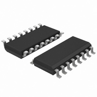
HEF4511BT,652 NXP Semiconductors, HEF4511BT,652 Datasheet - Page 2

HEF4511BT,652
Manufacturer Part Number
HEF4511BT,652
Description
IC BCD-7 SEG DECODER/DRVR 16SOIC
Manufacturer
NXP Semiconductors
Datasheets
1.HEF4046BT652.pdf
(26 pages)
2.HEF4511BP652.pdf
(19 pages)
3.HEF4511BP652.pdf
(11 pages)
Specifications of HEF4511BT,652
Package / Case
16-SOIC (3.9mm Width)
Display Type
LED
Configuration
7 Segment
Interface
BCD
Voltage - Supply
3 V ~ 15 V
Operating Temperature
-40°C ~ 85°C
Mounting Type
Surface Mount
Product
Latch/Decoder/Driver
Logic Family
HE4000B
Number Of Lines (input / Output)
7.0 / 7.0
Propagation Delay Time
120 ns
Supply Voltage (max)
15 V
Supply Voltage (min)
3 V
Maximum Operating Temperature
+ 85 C
Minimum Operating Temperature
- 40 C
Mounting Style
SMD/SMT
Number Of Input Lines
7.0
Number Of Output Lines
7.0
Lead Free Status / RoHS Status
Lead free / RoHS Compliant
Current - Supply
-
Digits Or Characters
-
Lead Free Status / Rohs Status
Lead free / RoHS Compliant
Other names
568-3125-5
933373180652
HEF4511BTD
933373180652
HEF4511BTD
Philips Semiconductors
DESCRIPTION
The HEF4511B is a BCD to 7-segment
latch/decoder/driver with four address inputs (D
an active LOW latch enable input (EL), an active LOW
ripple blanking input (BI), an active LOW lamp test input
(LT), and seven active HIGH n-p-n bipolar transistor
segment outputs (O
January 1995
BCD to 7-segment latch/decoder/driver
Fig.3 Schematic diagram of output stage.
Fig.1 Functional diagram.
a
to O
g
).
A
to D
D
),
2
When EL is LOW, the state of the segment outputs (O
O
When EL goes HIGH, the last data present on D
D
remain stable. When LT is LOW, all the segment outputs
are HIGH independent of all other input conditions. With
LT HIGH, a LOW on BI forces all segment outputs LOW.
The inputs LT and BI do not affect the latch circuit.
PINNING
FAMILY DATA, I
See Family Specifications
HEF4511BP(N):
HEF4511BD(F):
HEF4511BT(D):
( ): Package Designator North America
D
EL
BI
LT
O
D
g
A
a
) is determined by the data on D
are stored in the latches and the segment outputs
Fig.4
to D
to O
D
g
Segment
designation.
address (data) inputs
latch enable input (active LOW)
ripple blanking input (active LOW)
lamp test input (active LOW)
segment outputs
DD
Fig.2 Pinning diagram.
LIMITS category MSI
16-lead DIL; plastic (SOT38-1)
16-lead DIL; ceramic (cerdip) (SOT74)
16-lead SO; plastic (SOT109-1)
Product specification
A
to D
HEF4511B
D
.
A
MSI
to
a
to


