TC14433ELI Microchip Technology, TC14433ELI Datasheet - Page 8
TC14433ELI
Manufacturer Part Number
TC14433ELI
Description
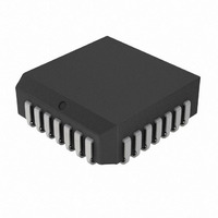
IC ADC 3 1/2 DIGIT 28PLCC
Manufacturer
Microchip Technology
Specifications of TC14433ELI
Display Type
LED
Configuration
7 Segment
Interface
BCD
Digits Or Characters
A/D 3.5 Digits
Current - Supply
1.8mA
Voltage - Supply
4.5 V ~ 8 V
Operating Temperature
-40°C ~ 85°C
Mounting Type
Surface Mount
Package / Case
28-PLCC
Lead Free Status / RoHS Status
Lead free / RoHS Compliant
Available stocks
Company
Part Number
Manufacturer
Quantity
Price
Company:

Part Number:
TC14433ELI
Manufacturer:
MICROCHIP
Quantity:
12 000
Company:
Part Number:
TC14433ELI
Manufacturer:
Microchip Technology
Quantity:
10 000
Company:
Part Number:
TC14433ELI713
Manufacturer:
MICROCHIP
Quantity:
12 000
Company:
Part Number:
TC14433ELI713
Manufacturer:
Microchip Technology
Quantity:
10 000


TC14433/A
4.0
The TC14433 CMOS IC becomes a modified dual-
slope A/D with a minimum of external components.
This IC has the customary CMOS digital logic circuitry,
as well as CMOS analog circuitry. It provides the user
with digital functions such as (counters, latches,
multiplexers),
(operational amplifiers and comparators) on a single
chip. Refer to the Functional Block diagram,
Features of the TC14433/A include auto-zero, high
input impedances and auto-polarity. Low power
consumption and a wide range of power supply
voltages are also advantages of this CMOS device.
The system’s auto-zero function compensates for the
offset voltage of the internal amplifiers and compara-
tors. In this “ratiometric system,” the output reading is
the ratio of the unknown voltage to the reference
voltage, where a ratio of 1 is equal to the maximum
count of 1999. It takes approximately 16,000 clock
periods to complete one conversion cycle. Each
conversion cycle may be divided into 6 segments.
Figure 4-1
for both positive and negative inputs.
i
FIGURE 4-1:
Pin 6.
DS21394D-page 8
Time
Segment
Number
DETAILED DESCRIPTION
Start
shows the conversion cycle in 6 segments
1
and
2
3
Integrator Waveforms at
analog
V
X
4
functions
5
V
X
6
End
Typical
Positive
Input Voltage
Typical
Negative
Input Voltage
Figure
such
4-3.
as
Segment 1 – The offset capacitor (C
sates for the input offset voltages of the buffer and
integrator amplifiers, is charged during this period.
However, the integrator capacitor is shorted. This
segment requires 4000 clock periods.
Segment 2 – During this segment, the integrator output
decreases to the comparator threshold voltage. At this
time, a number of counts equivalent to the input offset
voltage of the comparator is stored in the offset latches
for later use in the auto-zero process. The time for this
segment is variable and less than 800 clock periods.
Segment 3 – This segment of the conversion cycle is
the same as Segment 1.
Segment 4 – Segment 4 is an up going ramp cycle with
the unknown input voltage (V
integrator.
configuration of the analog section of the TC14433.
The actual configuration of the analog section is
dependent upon the polarity of the input voltage during
the previous conversion cycle.
FIGURE 4-2:
of the Analog Section During Segment 4 of the
Timing Cycle
Segment 5 – This segment is a down-going ramp
period with the reference voltage as the input to the
integrator. Segment 5 of the conversion cycle has a
time equal to the number of counts stored in the offset
storage latches during Segment 2. As a result, the
system zeros automatically.
Segment 6 – This is an extension of Segment 5. The
time period for this portion is 4000 clock periods. The
results of the A/D conversion cycle are determined in
this portion of the conversion cycle.
V
X
Buffer
+
–
Figure 4-2
R
1
Equivalent Circuit Diagrams
© 2008 Microchip Technology Inc.
shows
Integrator
+
–
C
X
1
as the input to the
O
), which compen-
the
Comparator
+
–
equivalent
Related parts for TC14433ELI
Image
Part Number
Description
Manufacturer
Datasheet
Request
R

Part Number:
Description:
Manufacturer:
Microchip Technology Inc.
Datasheet:
Part Number:
Description:
Manufacturer:
Microchip Technology Inc.
Datasheet:
Part Number:
Description:
Manufacturer:
Microchip Technology Inc.
Datasheet:
Part Number:
Description:
Manufacturer:
Microchip Technology Inc.
Datasheet:
Part Number:
Description:
Manufacturer:
Microchip Technology Inc.
Datasheet:
Part Number:
Description:
Manufacturer:
Microchip Technology Inc.
Datasheet:
Part Number:
Description:
Manufacturer:
Microchip Technology Inc.
Datasheet:
Part Number:
Description:
Manufacturer:
Microchip Technology Inc.
Datasheet: