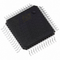
STFPC311BTR STMicroelectronics, STFPC311BTR Datasheet - Page 6

STFPC311BTR
Manufacturer Part Number
STFPC311BTR
Description
IC CTRL/DRIVER FRONT PNL 52-PQFP
Manufacturer
STMicroelectronics
Datasheet
1.STFPC311BTR.pdf
(39 pages)
Specifications of STFPC311BTR
Display Type
Vacuum Fluorescent (VF)
Interface
Serial
Current - Supply
5mA
Voltage - Supply
3 V ~ 33.3 V
Operating Temperature
-40°C ~ 85°C
Mounting Type
Surface Mount
Package / Case
52-MQFP, 52-PQFP
Maximum Operating Temperature
+ 85 C
Maximum Clock Frequency
1 MHz
Maximum Output Current
25 mA
Maximum Power Dissipation
1200 mA
Minimum Operating Temperature
- 40 C
Mounting Style
SMD/SMT
For Use With
497-8394 - BOARD DEMO STFPC311/ST72264497-6454 - BOARD EVAL BASED ON STFPC311
Lead Free Status / RoHS Status
Lead free / RoHS Compliant
Configuration
-
Digits Or Characters
-
Lead Free Status / Rohs Status
Details
Other names
497-6107-2
Available stocks
Company
Part Number
Manufacturer
Quantity
Price
Company:
Part Number:
STFPC311BTR
Manufacturer:
TI
Quantity:
200
Company:
Part Number:
STFPC311BTR
Manufacturer:
STMicroelectronics
Quantity:
10 000
Part Number:
STFPC311BTR
Manufacturer:
ST
Quantity:
20 000
2 Pin connection
2.1
Table 1.
Note: 1 For a detailed behavioral description of these pins, refer to the “STFPC311 Timing Power
6/39
14 to 25
27 to 34
35 to 37
6, 13,38
40 to 44
Pin Nº
12, 26
49-52
2, 3
8, 9
5S
10
39
45
46
47
48
1
4
7
1
Pin description
Stand-by Sequencer Flow-Chart”. See
to SEG20/GRID9
GRID8 to GRID6
GRID5 to GRID1
SEG13/GRID16
Pin description
SEG1/KS1 to
SEG12/KS12
LED1, LED2,
KEY1, KEY2
LED3, LED4
IR_DATA_IN
SW1, SW2
Symbol
READY
MUTE
OSC
GND
D
TBY
STB
CLK
V
V
NC
D
OUT
DD
SS
IN
POWER
POWER
POWER
Type
O
O
O
O
O
O
O
O
O
I
I
I
I
I
I
I
I
This is the oscillator input pin. Connect this pin to an external resistor.
Remote control input. Feeds the IR data from photodiode to this pin.
General purpose switch input ports.
High level indicates mute status for audio. Low level indicates normal
working.Note 1
there is a typo. Pin5 and name is STBY. Standby output to put the MCU
in low power mode.
It is a command to the main power board. High level indicates stand-by
status. Low level indicates normal working.
Connect this pin to system GND.
Input data to these pins from external keyboard are latched at end of
the display cycle (maximum keyboard size is 12 x 2).
High level on this pin means that main board chip has been working
normally.Note 1
pull-down resistor on this input.
Segment output pins (dual function as key source).
V
These pins are selectable for segment or grid driving.
Grid output pins.
3.3V ± 0.3V Core main supply voltage.
Not used. Left unconnected.
Grid output pins.
Initializes the serial interface at the rising or falling edge to make the
STFPC31 wait for reception of command. The data input after the falling
edge of STB is processed as a command. While the command data is
processed, current processing is stopped, and the serial interface is
initialized. While STB is high, CLK is ignored and any instruction from
the MCU is neglected.
Reads serial data at the rising edge, and outputs data at the falling
edge.
Inputs serial data at the rising edge of the shift clock, starting from the
lower bit.
Outputs serial data at the faling edge of the shift clock, starting from the
lower bit. This is the N-channel opendrain output pin.
CMOS outputs (20mA, max).
FD
outputs high voltage pull-down level. V
Table 6 on page 12
This pin should never float. It is recommended have a
Name and function
DD
Note 1
--33.3V max.
STFPC311


