MC14489BPE Freescale Semiconductor, MC14489BPE Datasheet - Page 4
MC14489BPE
Manufacturer Part Number
MC14489BPE
Description
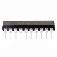
IC LED DRIVER 5-CH CMOS 20-DIP
Manufacturer
Freescale Semiconductor
Datasheet
1.MC14489BPE.pdf
(22 pages)
Specifications of MC14489BPE
Display Type
LED
Configuration
7 Segment
Interface
Serial
Current - Supply
5.5mA
Voltage - Supply
4.5 V ~ 5.5 V
Operating Temperature
-40°C ~ 130°C
Mounting Type
Through Hole
Package / Case
20-DIP (0.300", 7.62mm)
Number Of Digits
5
Number Of Segments
40
Low Level Output Current
200 uA
High Level Output Current
17500 uA
Operating Supply Voltage
4.5 V to 5.5 V
Maximum Supply Current
1500 uA
Maximum Operating Temperature
+ 130 C
Mounting Style
Through Hole
Minimum Operating Temperature
- 40 C
Lead Free Status / RoHS Status
Lead free / RoHS Compliant
Digits Or Characters
-
Lead Free Status / Rohs Status
Lead free / RoHS Compliant
Available stocks
Company
Part Number
Manufacturer
Quantity
Price

Part Number:
MC14489BPE
Manufacturer:
FREESCALE
Quantity:
20 000


* See Thermal Considerations section.
MC14489B
4
AC ELECTRICAL CHARACTERISTICS
TIMING REQUIREMENTS
** For a high–speed 8–Clock access, t h for Enable is determined as follows:
* See Thermal Considerations section.
Symbol
Symbol
t su , t h ,
where t h is in ns and f clk is in MHz.
NOTES:
t su , t h
t PLH ,
t TLH ,
t w(H)
t PHL
t THL
t w(L)
t r , t f
t rec
f clk
C in
f R
t w
V DD = 3 to 4.5 V, f clk > 1.78 MHz: t h = 4350 – (7500/f clk )
V DD = 4.5 to 5.5 V, f clk > 2.34 MHz: t h = 3300 – (7500/f clk )
1. This restriction does NOT apply for f clk rates less than those listed above. For “slow” f clk rates, use the t h limits in the above table.
2. This restriction does NOT apply for an access involving more than 8 Clocks. For > 8 Clocks, use the t h limits in the above table.
Serial Data Clock Frequency, Single Device or Cascaded Devices
NOTE: Refer to Clock t w below
Maximum Propagation Delay, Clock to Data Out
Maximum Output Transistion Time, Data Out
Refresh Rate — Bank 1 through Bank 5
Maximum Input Capacitance — Data In, Clock, Enable
Minimum Setup and Hold Times, Data In versus Clock
Minimum Setup, Hold, ** and Recovery Times, Enable versus Clock
Minimum Active–Low Pulse Width, Enable
Minimum Inactive–High Pulse Width, Enable
Minimum Pulse Width, Clock
Maximum Input Rise and Fall Times — Data In, Clock, Enable
(Figure 1)
(Figures 1 and 5)
(Figures 1 and 5)
(Figures 2 and 6)
(Figure 3)
(Figure 4)
(Figure 4)
(Figure 4)
(Figure 1)
(Figure 1)
(T J = – 40 to 130 C*, Input t r = t f = 10 ns unless otherwise indicated
(T J = – 40 to 130 C*, C L = 50 pF, Input t r = t f = 10 ns)
Parameter
Parameter
)
V DD
V DD
3.0
4.5
5.5
3.0
4.5
5.5
3.0
4.5
5.5
3.0
4.5
5.5
3.0
4.5
5.5
3.0
4.5
5.5
3.0
4.5
5.5
3.0
4.5
5.5
3.0
4.5
5.5
3.0
4.5
5.5
—
V
V
Guaranteed
Guaranteed
700 to 1900
700 to 1900
dc to 3.0
dc to 4.0
dc to 4.0
Limit
Limit
140
150
100
100
300
150
150
167
125
125
NA
4.5
3.4
3.4
80
80
70
50
50
10
50
40
40
1
1
1
MOTOROLA
MHz
Unit
Unit
ms
Hz
pF
ns
ns
ns
ns
ns
ns
s
Related parts for MC14489BPE
Image
Part Number
Description
Manufacturer
Datasheet
Request
R

Part Number:
Description:
Multi-character Display/lamp Driver
Manufacturer:
Freescale Semiconductor, Inc
Datasheet:

Part Number:
Description:
CONTACTOR, 1NO, 110VAC, 14A, DIN RAIL
Manufacturer:
IMO PRECISION CONTROLS
Datasheet:
Part Number:
Description:
CONTACTOR, 1NO, 230VAC, 14A, DIN RAIL
Manufacturer:
IMO PRECISION CONTROLS
Datasheet:
Part Number:
Description:
CONTACTOR, 1NO, 24VAC, 14A, DIN RAIL
Manufacturer:
IMO PRECISION CONTROLS
Datasheet:
Part Number:
Description:
Manufacturer:
Freescale Semiconductor, Inc
Datasheet:
Part Number:
Description:
Manufacturer:
Freescale Semiconductor, Inc
Datasheet:
Part Number:
Description:
Manufacturer:
Freescale Semiconductor, Inc
Datasheet:
Part Number:
Description:
Manufacturer:
Freescale Semiconductor, Inc
Datasheet:
Part Number:
Description:
Manufacturer:
Freescale Semiconductor, Inc
Datasheet:
Part Number:
Description:
Manufacturer:
Freescale Semiconductor, Inc
Datasheet:
Part Number:
Description:
Manufacturer:
Freescale Semiconductor, Inc
Datasheet:
Part Number:
Description:
Manufacturer:
Freescale Semiconductor, Inc
Datasheet:
Part Number:
Description:
Manufacturer:
Freescale Semiconductor, Inc
Datasheet:
Part Number:
Description:
Manufacturer:
Freescale Semiconductor, Inc
Datasheet:
Part Number:
Description:
Manufacturer:
Freescale Semiconductor, Inc
Datasheet: