MC14489BPE Freescale Semiconductor, MC14489BPE Datasheet - Page 3
MC14489BPE
Manufacturer Part Number
MC14489BPE
Description
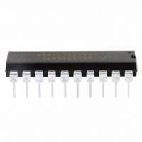
IC LED DRIVER 5-CH CMOS 20-DIP
Manufacturer
Freescale Semiconductor
Datasheet
1.MC14489BPE.pdf
(22 pages)
Specifications of MC14489BPE
Display Type
LED
Configuration
7 Segment
Interface
Serial
Current - Supply
5.5mA
Voltage - Supply
4.5 V ~ 5.5 V
Operating Temperature
-40°C ~ 130°C
Mounting Type
Through Hole
Package / Case
20-DIP (0.300", 7.62mm)
Number Of Digits
5
Number Of Segments
40
Low Level Output Current
200 uA
High Level Output Current
17500 uA
Operating Supply Voltage
4.5 V to 5.5 V
Maximum Supply Current
1500 uA
Maximum Operating Temperature
+ 130 C
Mounting Style
Through Hole
Minimum Operating Temperature
- 40 C
Lead Free Status / RoHS Status
Lead free / RoHS Compliant
Digits Or Characters
-
Lead Free Status / Rohs Status
Lead free / RoHS Compliant
Available stocks
Company
Part Number
Manufacturer
Quantity
Price

Part Number:
MC14489BPE
Manufacturer:
FREESCALE
Quantity:
20 000


* See Thermal Considerations section.
MOTOROLA
ELECTRICAL CHARACTERISTICS
V DD (stby)
I DD , I SS
Symbol
V Hys
V OH
V DD
V OL
i OH
R on
V IH
i OL
I OZ
V IL
I ss
I in
Power Supply Voltage Range of LED Drive Circuitry
Minimum Standby Voltage
Maximum Low–Level Input Voltage
Minimum High–Level Input Voltage
Minimum Hysteresis Voltage
Maximum Low–Level Output Voltage
Minimum High–Level Output Voltage
Maximum Input Leakage Current
Minimum Sinking Current
Peak Sourcing Current — See Figure 7 for currents up to
Maximum Output Leakage Current
Maximum ON Resistance
Maximum Quiescent Supply Current
Maximum RMS Operating Supply Current
See Pin Descriptions.)
(Data In, Clock, Enable)
(Data In, Clock, Enable)
(Data In, Clock, Enable)
(Data Out)
(Data Out)
(Data In Clock Enable)
(Data In, Clock, Enable)
(a, b, c, d, e, f, g, h)
35 mA (a, b, c, d, e, f, g, h)
(Bank 1 Bank 2 Bank 3 Bank 4 Bank 5)
(Bank 1, Bank 2, Bank 3, Bank 4, Bank 5)
(Bank 1, Bank 2, Bank 3, Bank 4, Bank 5)
(The V SS leg does not contain the Rx current component.
Parameter
(Voltages Referenced to V SS , T J = – 40 to 130 C* unless otherwise indicated)
Bits Retained in Display and
Configuration Registers, Data
Port Fully Functional
I out = 20 A
I out = 1.3 mA
I out = – 20 A
I out = – 800 A
V in = V DD or V SS
V in = V DD or V SS ,
T J = 25 C only
V out = 1.0 V
Rx = 2.0 k , V out = 3.0 V,
Dimmer Bit = High
Rx = 2.0 k , V out = 3.0 V,
Dimmer Bit = Low
V out = V DD (FET Leakage)
V out = V DD (FET Leakage),
T J = 25 C only
V out = V SS (Protection Diode
Leakage)
I out = 0 to 200 mA
Device in Low–Power Mode,
V in = V SS or V DD , Rx in
Place, Outputs Open
Same as Above, T J = 25 C
Device NOT in Low–Power
Mode, V in = V SS or V DD ,
Outputs Open
Test Condition
V DD
3.0
5.5
3.0
5.5
3.0
5.5
3.0
5.5
4.5
3.0
5.5
4.5
5.5
5.5
4.5
5.0
5.0
5.5
5.5
5.5
5.0
5.5
5.5
5.5
—
—
V
Guaranteed
13 to 17.5
4.5 to 5.5
6 to 9
Limit
100
3.0
0.9
1.65
2.1
3.85
0.2
0.4
0.1
0.1
0.4
2.9
5.4
4.1
0.2
1.5
50
10
20
2.0
0.1
1
1
MC14489B
Unit
mA
mA
mA
V
V
V
V
V
V
V
A
A
A
3
Related parts for MC14489BPE
Image
Part Number
Description
Manufacturer
Datasheet
Request
R

Part Number:
Description:
Multi-character Display/lamp Driver
Manufacturer:
Freescale Semiconductor, Inc
Datasheet:

Part Number:
Description:
CONTACTOR, 1NO, 110VAC, 14A, DIN RAIL
Manufacturer:
IMO PRECISION CONTROLS
Datasheet:
Part Number:
Description:
CONTACTOR, 1NO, 230VAC, 14A, DIN RAIL
Manufacturer:
IMO PRECISION CONTROLS
Datasheet:
Part Number:
Description:
CONTACTOR, 1NO, 24VAC, 14A, DIN RAIL
Manufacturer:
IMO PRECISION CONTROLS
Datasheet:
Part Number:
Description:
Manufacturer:
Freescale Semiconductor, Inc
Datasheet:
Part Number:
Description:
Manufacturer:
Freescale Semiconductor, Inc
Datasheet:
Part Number:
Description:
Manufacturer:
Freescale Semiconductor, Inc
Datasheet:
Part Number:
Description:
Manufacturer:
Freescale Semiconductor, Inc
Datasheet:
Part Number:
Description:
Manufacturer:
Freescale Semiconductor, Inc
Datasheet:
Part Number:
Description:
Manufacturer:
Freescale Semiconductor, Inc
Datasheet:
Part Number:
Description:
Manufacturer:
Freescale Semiconductor, Inc
Datasheet:
Part Number:
Description:
Manufacturer:
Freescale Semiconductor, Inc
Datasheet:
Part Number:
Description:
Manufacturer:
Freescale Semiconductor, Inc
Datasheet:
Part Number:
Description:
Manufacturer:
Freescale Semiconductor, Inc
Datasheet:
Part Number:
Description:
Manufacturer:
Freescale Semiconductor, Inc
Datasheet: