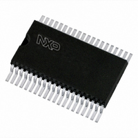
PCF8566T/1,112 NXP Semiconductors, PCF8566T/1,112 Datasheet - Page 23

PCF8566T/1,112
Manufacturer Part Number
PCF8566T/1,112
Description
IC LCD DVR UNVRSL LOW-MUX 40VSOP
Manufacturer
NXP Semiconductors
Datasheet
1.PCF8566T1118.pdf
(48 pages)
Specifications of PCF8566T/1,112
Package / Case
40-VSOP
Display Type
LCD
Configuration
7 Segment + DP, 14 Segment (24 Segment)
Interface
I²C
Current - Supply
30µA
Voltage - Supply
2.5 V ~ 6 V
Operating Temperature
-40°C ~ 85°C
Mounting Type
Surface Mount
Number Of Digits
12
Number Of Segments
96
Maximum Clock Frequency
315 KHz
Operating Supply Voltage
2.5 V to 6 V
Maximum Power Dissipation
400 mW
Maximum Operating Temperature
+ 85 C
Attached Touch Screen
No
Maximum Supply Current
90 uA
Minimum Operating Temperature
- 40 C
Lead Free Status / RoHS Status
Lead free / RoHS Compliant
Digits Or Characters
-
Lead Free Status / Rohs Status
Lead free / RoHS Compliant
Other names
568-5030
935278688112
PCF8566T/1,112
PCF8566TD
PCF8566TD
935278688112
PCF8566T/1,112
PCF8566TD
PCF8566TD
NXP Semiconductors
PCF8566_7
Product data sheet
Two displays controlled by PCF8566 can be recognized on the same I
allows:
The I
condition (S) from the I
addresses. All PCF8566s with the same SA0 level acknowledge in parallel to the slave
address. All PCF8566s with the alternative SA0 level ignore the whole I
After acknowledgement, one or more command bytes (m) follow which define the status of
the addressed PCF8566s. The last command byte is tagged with a cleared most
significant bit, the continuation bit C. The command bytes are also acknowledged by all
addressed PCF8566s on the bus.
After the last command byte, a series of display data bytes (n) may follow. These display
bytes are stored in the display RAM at the address specified by the data pointer and the
subaddress counter. Both data pointer and subaddress counter are automatically updated
and the data is directed to the intended PCF8566 device.
The acknowledgement after each byte is made only by the (A0, A1 and A2) addressed
PCF8566. After the last display byte, the I
Fig 16. Slave address structure
Fig 17. I
•
•
Up to 16 PCF8566s on the same I
Section
The use of two types of LCD multiplex on the same I
2
C-bus protocol is shown in
S
2
C-bus protocol
13)
0 1 1 1 1 1
slave address
1 byte
Rev. 07 — 25 February 2009
2
C-bus master which is followed by one of the PCF8566 slave
S
A
0
R/W
0 A C
Figure
acknowledge by
0 1 1 1 1 1
all addressed
m
PCF8566s
2
slave address
COMMAND
C-bus for very large LCD applications (see
1 byte(s)
17. The sequence is initiated with a START
2
1 byte
Universal LCD driver for low multiplex rates
C-bus master issues a STOP condition (P).
001aai455
S
A
0
R/W
A
0
DISPLAY DATA
2
n > 0 byte(s)
C-bus
by A0, A1 and A2
update data pointers
subaddress counter
PCF8566 only
and if necessary,
acknowledge
selected
2
PCF8566
C-bus which
© NXP B.V. 2009. All rights reserved.
2
A
C-bus transfer.
P
mgg390
23 of 48


