MAX745EAP+ Maxim Integrated Products, MAX745EAP+ Datasheet - Page 8
MAX745EAP+
Manufacturer Part Number
MAX745EAP+
Description
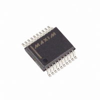
IC BATTERY CHARGER LI+ 20-SSOP
Manufacturer
Maxim Integrated Products
Datasheet
1.MAX745EAP.pdf
(8 pages)
Specifications of MAX745EAP+
Function
Charge Management
Battery Type
Lithium-Ion (Li-Ion)
Voltage - Supply
6 V ~ 24 V
Operating Temperature
-40°C ~ 85°C
Mounting Type
Surface Mount
Package / Case
20-SSOP
Output Voltage
5.4 V
Operating Supply Voltage
6 V to 24 V
Supply Current
4 mA
Maximum Operating Temperature
+ 85 C
Minimum Operating Temperature
- 40 C
Mounting Style
SMD/SMT
Lead Free Status / RoHS Status
Lead free / RoHS Compliant


The MAX745 drives external N-channel MOSFETs to
switch the input source generating the battery voltage or
current. Since the high-side N-channel MOSFET’s gate
must be driven to a voltage higher than the input source
voltage, a charge pump is used to generate such a volt-
age. The capacitor (C7) charges through D2 to approxi-
mately 5V when the synchronous rectifier (M1B) turns on
(Figure 1). Since one side of C7 is connected to LX (the
source of M1A), the high-side driver (DHI) drives the gate
up to the voltage at BST, which is greater than the input
voltage while the high-side MOSFET is on.
The synchronous rectifier (M1B) behaves like a diode
but has a smaller voltage drop, improving efficiency. A
small dead time is added between the time when the
high-side MOSFET is turned off and when the synchro-
nous rectifier is turned on, and vice versa. This
prevents crowbar currents during switching transitions.
Place a Schottky rectifier from LX to ground (D1, across
M1B’s drain and source) to prevent the synchronous
rectifier’s body diode from conducting during the dead
time. The body diode typically has slower switching-
recovery times, so allowing it to conduct degrades
efficiency. D1 can be omitted if efficiency is not a
concern, but the resulting increased power dissipation
in the synchronous rectifier must be considered.
Since the BST capacitor is charged while the synchro-
nous rectifier is on, the synchronous rectifier may not be
replaced by a rectifier. The BST capacitor will not fully
charge without the synchronous rectifier, leaving the high-
side MOSFET with insufficient gate drive to turn on.
However, the synchronous rectifier can be replaced with
a small MOSFET (such as a 2N7002) to guarantee that
the BST capacitor is allowed to charge. In this case, the
majority of the high charging currents are carried by D1,
and not by the synchronous rectifier.
The MAX745 uses an internal low-dropout linear regula-
tor to create a 5.4V power supply (VL), which powers its
internal circuitry. The VL regulator can supply up to
25mA. Since 4mA of this current powers the internal cir-
cuitry, the remaining 21mA can be used for external cir-
cuitry. MOSFET gate-drive current comes from VL,
which must be considered when drawing current for
other functions. To estimate the current required to drive
the MOSFETs, multiply the sum of the MOSFET gate
charges by the switching frequency (typically 300kHz).
Bypass VL with a 4.7
The MAX745 internal 4.2V reference voltage must be
bypassed with a 0.1
Switch-Mode Lithium-Ion
Battery Charger
8
_______________________________________________________________________________________
Internal Regulator and Reference
µ
µ
F or greater capacitor.
F capacitor to ensure stability.
MOSFET Drivers
The input voltage to the charger circuit must be greater
than the maximum battery voltage by approximately 2V
so the charger can regulate the voltage properly. The
input voltage can have a large AC-ripple component
when operating from a wall cube. The voltage at the low
point of the ripple waveform must still be approximately
2V greater than the maximum battery voltage.
Using components as indicated in Figure 1, the minimum
input voltage can be determined by the following formula:
where: V
TRANSISTOR COUNT: 1695
SUBSTRATE CONNECTED TO GND
___________________Chip Information
__________________Pin Configuration
TOP VIEW
V
IN
x
V
(typically 0.4V to 0.5V);
I
R
MOSFET M1A’s on-resistance;
R
R1 is the current-sense resistor R1’s value.
CHG
[V
IN
D6
DS(ON)
L
THM/SHDN
is the the inductor’s series resistance;
BATT
is the input voltage;
is the voltage drop across D6
is the charging current;
DCIN
VADJ
IBAT
SETI
GND
CCV
REF
CCI
VL
+ V
is the high-side
10
1
2
3
4
5
6
7
8
9
D6
+ I
MAX745
SSOP
Minimum Input Voltage
0.89
CHG
( R
DS(ON)
20
19
18
17
16
15
14
13
12
11
BST
LX
DHI
DLO
PGND
CS
STATUS
CELL0
CELL1
BATT
+ R
L
+ R1)]
Related parts for MAX745EAP+
Image
Part Number
Description
Manufacturer
Datasheet
Request
R

Part Number:
Description:
MAX7528KCWPMaxim Integrated Products [CMOS Dual 8-Bit Buffered Multiplying DACs]
Manufacturer:
Maxim Integrated Products
Datasheet:
Part Number:
Description:
Single +5V, fully integrated, 1.25Gbps laser diode driver.
Manufacturer:
Maxim Integrated Products
Datasheet:
Part Number:
Description:
Single +5V, fully integrated, 155Mbps laser diode driver.
Manufacturer:
Maxim Integrated Products
Datasheet:
Part Number:
Description:
VRD11/VRD10, K8 Rev F 2/3/4-Phase PWM Controllers with Integrated Dual MOSFET Drivers
Manufacturer:
Maxim Integrated Products
Datasheet:
Part Number:
Description:
Highly Integrated Level 2 SMBus Battery Chargers
Manufacturer:
Maxim Integrated Products
Datasheet:
Part Number:
Description:
Current Monitor and Accumulator with Integrated Sense Resistor; ; Temperature Range: -40°C to +85°C
Manufacturer:
Maxim Integrated Products
Part Number:
Description:
TSSOP 14/A�/RS-485 Transceivers with Integrated 100O/120O Termination Resis
Manufacturer:
Maxim Integrated Products
Part Number:
Description:
TSSOP 14/A�/RS-485 Transceivers with Integrated 100O/120O Termination Resis
Manufacturer:
Maxim Integrated Products
Part Number:
Description:
QFN 16/A�/AC-DC and DC-DC Peak-Current-Mode Converters with Integrated Step
Manufacturer:
Maxim Integrated Products
Part Number:
Description:
TDFN/A/65V, 1A, 600KHZ, SYNCHRONOUS STEP-DOWN REGULATOR WITH INTEGRATED SWI
Manufacturer:
Maxim Integrated Products
Part Number:
Description:
Integrated Temperature Controller f
Manufacturer:
Maxim Integrated Products
Part Number:
Description:
SOT23-6/I�/45MHz to 650MHz, Integrated IF VCOs with Differential Output
Manufacturer:
Maxim Integrated Products
Part Number:
Description:
SOT23-6/I�/45MHz to 650MHz, Integrated IF VCOs with Differential Output
Manufacturer:
Maxim Integrated Products
Part Number:
Description:
EVALUATION KIT/2.4GHZ TO 2.5GHZ 802.11G/B RF TRANSCEIVER WITH INTEGRATED PA
Manufacturer:
Maxim Integrated Products
Part Number:
Description:
QFN/E/DUAL PCIE/SATA HIGH SPEED SWITCH WITH INTEGRATED BIAS RESISTOR
Manufacturer:
Maxim Integrated Products
Datasheet: