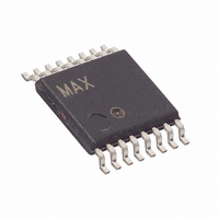
DS2762BE+025 Maxim Integrated Products, DS2762BE+025 Datasheet - Page 17

DS2762BE+025
Manufacturer Part Number
DS2762BE+025
Description
IC MON BATT LI-ION HP 16-TSSOP
Manufacturer
Maxim Integrated Products
Datasheet
1.DS2762BE025TR.pdf
(25 pages)
Specifications of DS2762BE+025
Function
Battery Monitor
Battery Type
Lithium-Ion (Li-Ion)
Voltage - Supply
2.5 V ~ 5.5 V
Operating Temperature
-40°C ~ 85°C
Mounting Type
Surface Mount
Package / Case
16-TSSOP
Product
Fuel Gauges
Operating Supply Voltage
2.5 V to 5.5 V
Supply Current
60 uA
Maximum Operating Temperature
+ 85 C
Minimum Operating Temperature
- 40 C
Charge Safety Timers
Yes
Mounting Style
SMD/SMT
Temperature Monitoring
Yes
Uvlo Start Threshold
2.6 V
Uvlo Stop Threshold
4.35 V
Lead Free Status / RoHS Status
Lead free / RoHS Compliant
EEPROM REGISTER
The format of the EEPROM register is shown in Figure 12. The function of each bit is described in detail in the
following paragraphs.
Figure 12. EEPROM Register Format
EEC—EEPROM Copy Flag. A 1 in this read-only bit indicates that a copy data command is in progress. While this
bit is high, writes to EEPROM addresses are ignored. A 0 in this bit indicates that data may be written to unlocked
EEPROM blocks.
LOCK—EEPROM Lock Enable. When this bit is 0, the lock command is ignored. Writing a 1 to this bit enables the
lock command. After the lock command is executed, the LOCK bit is reset to 0. The factory default is 0.
BL1—EEPROM Block 1 Lock Flag. A 1 in this read-only bit indicates that EEPROM block 1 (addresses 30 to 3F) is
locked (read-only) while a 0 indicates block 1 is unlocked (read/write).
BL0—EEPROM Block 0 Lock Flag. A 1 in this read-only bit indicates that EEPROM block 0 (addresses 20 to 2F) is
locked (read-only) while a 0 indicates block 0 is unlocked (read/write).
X—Reserved Bits.
SPECIAL FEATURE REGISTER
The format of the special feature register is shown in Figure 13. The function of each bit is described in detail in the
following paragraphs.
Figure 13. Special Feature Register Format
PS — PS Pin Latch. This bit latches a low state on the PS pin, and is cleared only by writing a 1 to this location.
Writing this bit to a 1 immediately upon reading of a 0 value is recommended.
PIO—PIO Pin Sense and Control. See the Programmable I/O section for details on this read/write bit.
MSTR—SWAP Master Status Bit. This bit indicates whether a device has been selected through the SWAP
command. Selection of this device through the SWAP command and the appropriate net address results in setting
this bit, indicating that this device is the master. A 0 signifies that this device is not the master.
X—Reserved Bits.
BIT 7
BIT 7
EEC
PS
LOCK
BIT 6
BIT 6
PIO
MSTR
BIT 5
BIT 5
X
BIT 4
BIT 4
ADDRESS 07
ADDRESS 08
X
X
17 of 25
BIT 3
BIT 3
X
X
BIT 2
BIT 2
X
X
BIT 1
BIT 1
BL1
X
BIT 0
BIT 0
BL0
X


