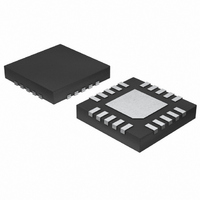
MAX17006BETP+ Maxim Integrated Products, MAX17006BETP+ Datasheet - Page 20

MAX17006BETP+
Manufacturer Part Number
MAX17006BETP+
Description
IC BATT CHARGER 1.2MHZ 20-TQFN
Manufacturer
Maxim Integrated Products
Specifications of MAX17006BETP+
Function
Charge Management
Battery Type
Multi-Chemistry
Voltage - Supply
8 V ~ 26 V
Operating Temperature
-40°C ~ 85°C
Mounting Type
Surface Mount
Package / Case
20-TQFN Exposed Pad
Lead Free Status / RoHS Status
Lead free / RoHS Compliant
1.2MHz Low-Cost,
High-Performance Chargers
For optimum size and inductor current ripple, choose
LIR
charge current and results in a good balance between
inductor size and efficiency. Higher inductor values
decrease the ripple current. Smaller inductor values
save cost but require higher saturation current capabili-
ties and degrade efficiency.
Inductor L1 must have a saturation current rating of at
least the maximum charge current plus 1/2 the ripple
current (ΔIL):
The ripple current is determined by:
The input capacitor must meet the ripple current
requirement (I
Nontantalum chemistries (ceramic, aluminum, or
OS-CON) are preferred due to their resilience to power-
up and surge currents:
The input capacitors should be sized so that the tem-
perature rise due to ripple current in continuous con-
duction does not exceed approximately 10°C. The
maximum ripple current occurs at 50% duty factor or
V
application of interest does not achieve the maximum
value, size the input capacitors according to the worst-
case conditions.
The output capacitor absorbs the inductor ripple cur-
rent and must tolerate the surge current delivered from
the battery when it is initially plugged into the charger.
As such, both capacitance and ESR are important
parameters in specifying the output capacitor as a filter
and to ensure the stability of the DC-to-DC converter
(see the Compensation section.) Beyond the stability
requirements, it is often sufficient to make sure that the
output capacitor’s ESR is much lower than the battery’s
ESR. Either tantalum or ceramic capacitors can be
used on the output. Ceramic devices are preferable
because of their good voltage ratings and resilience to
surge currents. Choose the output capacitor based on:
20
DCIN
MAX
______________________________________________________________________________________
I
= 2 x V
RMS
= 0.4, which sets the ripple current to 40% the
C
OUT
=
I
RMS
CHG
BATT
=
I
SAT
f
SW
) imposed by the switching currents.
×
, which equates to 0.5 x I
⎛
⎜
⎜
⎝
Output Capacitor Selection
Δ
= I
× ×
I
IL
Input Capacitor Selection
RIPPLE
8 Δ
V
CHG
BATT
=
k V
V
×
+ (1/2) ΔIL
BATT
4
×
L
IN
(
V
V
DCIN
2
DCIN
×
k
CAP BIAS
−
V
−
BATT
CHG
)
⎞
⎟
⎟
⎠
. If the
Choose k
rated ceramic capacitors.
For f
70mV, choose C
If the internal resistance of battery is close to the ESR of
the output capacitor, the voltage ripple is shared with
the battery and is less than calculated.
The input current limit should be set based on the cur-
rent capability of the AC adapter and the tolerance of
the input current limit. The upper limit of the input cur-
rent threshold should never exceed the adapter’s mini-
mum available output current. For example, if the
adapter’s output current rating is 5A ±10%, the input
current limit should be selected so that its upper limit is
less than 5A × 0.9 = 4.5A. Since the input current-limit
accuracy of the MAX17005/MAX17006/MAX17015 is
±3%, the typical value of the input current limit should
be set at 4.5A/1.03 ≈ 4.36A. The lower limit for input
current must also be considered. For chargers at the
low end of the spec, the input current limit for this
example could be 4.36A × 0.95 or approximately 4.14A.
Bypass DCIN with a 0.1μF ceramic to ground (Figure 1).
N1 and N2 protect the MAX17005/MAX17006/
MAX17015 when the DC power source input is reversed.
Bypass V
Good PCB layout is required to achieve specified noise
immunity, efficiency, and stable performance. The PCB
layout designer must be given explicit instructions—
preferably, a sketch showing the placement of the
power switching components and high current routing.
Refer to the PCB layout in the MAX17005/MAX17006/
MAX17015 evaluation kit for examples. A ground plane
is essential for optimum performance. In most applica-
tions, the circuit is located on a multilayer board, and
full use of the four or more copper layers is recom-
mended. Use the top layer for high-current connec-
tions, the bottom layer for quiet connections, and the
inner layers for an uninterrupted ground plane.
Use the following step-by-step guide:
1) Place the high-power connections first, with their
grounds adjacent:
a) Minimize the current-sense resistor trace lengths,
b) Minimize ground trace lengths in the high-current
SW
and ensure accurate current sensing with Kelvin
connections.
paths.
= 800kHz, I
CAP-BIAS
AA
, CSSP, and LDO as shown in Figure 1.
Applications Information
OUT
is a derating factor of 2 for typical 25V-
RIPPLE
Setting Input Current Limit
as 4.7μF.
Layout and Bypassing
= 1A, and to get ΔV
BATT
=


