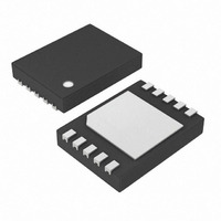
DS2782G-5+T&R Maxim Integrated Products, DS2782G-5+T&R Datasheet - Page 25

DS2782G-5+T&R
Manufacturer Part Number
DS2782G-5+T&R
Description
IC FUEL GAUGE STND-ALONE 10-TDFN
Manufacturer
Maxim Integrated Products
Datasheet
1.DS2782E.pdf
(28 pages)
Specifications of DS2782G-5+T&R
Function
Fuel, Gas Gauge/Monitor
Battery Type
Lithium-Ion (Li-Ion), Lithium-Polymer (Li-Pol)
Voltage - Supply
2.5 V ~ 5.5 V
Operating Temperature
-40°C ~ 85°C
Mounting Type
Surface Mount
Package / Case
10-TDFN Exposed Pad
Lead Free Status / RoHS Status
Lead free / RoHS Compliant
Acknowledge Bits
Each byte of a data transfer is acknowledged with an Acknowledge bit (A) or a No Acknowledge bit (N). Both the
master and the DS2782 slave generate acknowledge bits. To generate an Acknowledge, the receiving device must
pull SDA low before the rising edge of the acknowledge-related clock pulse (ninth pulse) and keep it low until SCL
returns low. To generate a No Acknowledge (also called NAK), the receiver releases SDA before the rising edge of
the acknowledge-related clock pulse and leaves SDA high until SCL returns low. Monitoring the acknowledge bits
allows for detection of unsuccessful data transfers. An unsuccessful data transfer can occur if a receiving device is
busy or if a system fault has occurred. In the event of an unsuccessful data transfer, the bus master should re-
attempt communication.
Data Order
A byte of data consists of 8 bits ordered most significant bit (msb) first. The least significant bit (lsb) of each byte is
followed by the Acknowledge bit. DS2782 registers composed of multi-byte values are ordered most significant
byte (MSB) first. The MSB of multi-byte registers is stored on even data memory addresses.
Slave Address
A bus master initiates communication with a slave device by issuing a START condition followed by a Slave
Address (SAddr) and the read/write (R/W) bit. When the bus is idle, the DS2782 continuously monitors for a
START condition followed by its slave address. When the DS2782 receives a slave address that matches the value
in its Programmable Slave Address register, it responds with an Acknowledge bit during the clock period following
the R/W bit. The 7-bit Programmable Slave Address register is factory programmed to 0110100. The slave address
can be re-programmed, refer to the Programmable Slave Address section for details.
Read/Write Bit
The R/W bit following the slave address determines the data direction of subsequent bytes in the transfer. R/W = 0
selects a write transaction, with the following bytes being written by the master to the slave. R/W = 1 selects a read
transaction, with the following bytes being read from the stave by the master.
Bus Timing
The DS2782 is compatible with any bus timing up to 400kHz. No special configuration is required to operate at any
speed.
2-Wire Command Protocols
The command protocols involve several transaction formats. The simplest format consists of the master writing the
START bit, slave address, R/W bit, and then monitoring the acknowledge bit for presence of the DS2782. More
complex formats such as the Write Data, Read Data and Function command protocols write data, read data and
execute device specific operations. All bytes in each command format require the slave or host to return an
Acknowledge bit before continuing with the next byte. Each function command definition outlines the required
transaction format. The following key applies to the transaction formats.
Table 4. 2-Wire Protocol Key
S
SAddr
FCmd
MAddr
Data
A
N
KEY
START bit
Slave Address (7-bit)
Function Command byte
Memory Address byte
Data byte written by master
Acknowledge bit - Master
No Acknowledge - Master
DESCRIPTION
25 of 28
Sr
W
R
P
Data
A
N
KEY
Repeated START
R/W bit = 0
R/W bit = 1
STOP bit
Data byte returned by slave
Acknowledge bit - Slave
No Acknowledge - Slave
DESCRIPTION


