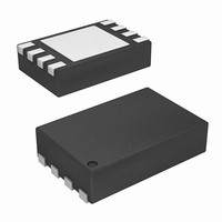
ISL9206ADRTZ-T Intersil, ISL9206ADRTZ-T Datasheet - Page 6

ISL9206ADRTZ-T
Manufacturer Part Number
ISL9206ADRTZ-T
Description
IC AUTHENTICATION DEVICE 8-TDFN
Manufacturer
Intersil
Series
FlexiHash+™r
Datasheet
1.ISL9206ADHZ-T.pdf
(17 pages)
Specifications of ISL9206ADRTZ-T
Function
Battery Authentication
Battery Type
Li-Ion, Li-Pol, NiMH
Voltage - Supply
2.6 V ~ 4.8 V
Operating Temperature
-25°C ~ 85°C
Mounting Type
Surface Mount
Package / Case
8-TDFN Exposed Pad
Lead Free Status / RoHS Status
Lead free / RoHS Compliant
function can be permanently disabled by clearing the 0-00[2]
bit (the ASLP bit in DCFG) during OTP ROM programming.
OTP ROM
The 16-Byte OTP ROM memory is based on EEPROM
technology and is incorporated into the ISL9206A for storage
of non-volatile information. OTP ROM contents (refer to
Table 8) can include, but are not limited to:
The memory can be written multiple times before two lock-out
bits (SLO[1:0] in DCFG, see Table 8) are set. The SLO[1] (bit
1) locks out the memory between 0-02 and 0-09 and the
SLO[0] (bit 0) locks out the memory between 0-0A to 0-0D.
These two bits can be set independently. Prior to lock-out, the
memory can be written and read directly through the XSD bus
interface. After lock-out, writing to all ROM addresses and
reading from secret code locations will be permanently
disabled after performing a reset cycle.
Writing to the EEPROM requires the supply voltage at the VDD
pin be maintained at a minimum of 2.8V. Failure to do so may
result in unreliable ROM programming or total write failure.
The OTP ROM must be written two bytes at a time, but 2, 4
or 16-Bytes of data can be read by the host in a single bus
transaction. Only even addresses are allowed in OTP ROM
read/write. A 16-Byte read with CRC allows the entire ROM
content to be quickly verified by simply checking the CRC
byte. The DTRM address stores the default trimming
parameters and is a read-only address. The DCFG and
DTRM (0-00 and 0-01 addresses) need to be written
simultaneously but the data to the DRTM address is ignored.
The OTP ROM writing process takes approximately 1.8ms
per two-bytes. While the write process is taking place, no bus
transaction is allowed. Attempting to access the ISL9206A
during an on-going write process will result in the device
ignoring the access instruction and issuing an interrupt to the
host. The OTP ROM programming is register based, and may
be performed at the pack manufacturer’s facility.
Device Control and Status
The ISL9206A has a control and a status register. The
control register can be read and written by the host but the
status register is read only. Both registers contain the device
configuration information (see Table 9). The status register
also contains the device status information that may lead to
an interrupt signal to the host.
Following a host-initiated power-on ‘break’ signal or soft
reset command, the ISL9206A will configure its default mode
of operation based on information stored within DCFG
address of the OTP ROM. The default configuration is
loaded into the master control (MSCR) and the status
1. Device default settings (address 0-00)
2. Factory programmed trim parameters (address 0-01)
3. Device authentication secrets (address 0-02 to 0-0D)
4. Pack information and ID (address 0-0E and 0-0F)
6
ISL9206A
(STAT) registers. Functions that are configured by OTP
ROM settings include:
The ISL9206A incorporates interrupt functions to allow the
host to be quickly informed of device status and error
conditions. Available interrupts are summarized in Table 1.
When an interrupt enable bit is set, a ’break’ command is
sent to the host whenever its corresponding interrupt status
bit is set. After this, the host should read the STAT register
immediately. If the following instruction frame from the host
does not access the STAT register, another ‘break’ will be
sent immediately after receiving the full instruction frame.
This process is repeated until the host reads from the STAT
register. Upon reading of the STAT register, all status bits will
be cleared.
Refer to Tables 14 and 15 for detailed explanations of the
interrupt functions.
FlexiHash+™ Engine
The FlexiHash+™ engine contains a 32-Bit highly non-linear
proprietary hash engine and three registers. Table 10 lists
the three registers. The 1-Byte secret selection (SESL)
register selects two sets of secret (32-Bit each) from the
OTP ROM to program the hash engine. The 4-Byte
challenge code register (CHLG) receives the challenge code
from the host through the XSD bus. Once the challenge
code is received, the hash engine generates a 1-Byte
authentication result code and stores in the AUTH register
for the host to read. Figure 5 shows the data flow of the
authentication process. The following sections describe the
authentication process and FlexiHash+™ encoding scheme
in detail.
THE DEVICE AUTHENTICATION PROCESS
To start an authentication process, the host sends a ‘break’
command to wake-up the ISL9206A. Then the host writes to
the SESL register to select the two sets of secrets to be used
for authentication code generation. After that, the host
generates a pseudo-random 4-Byte challenge code to input
into the CHLG register to initiate the authentication process.
Upon receiving the fourth byte of the challenge code, the
ISL9206A immediately starts computing the authentication
code. Once the computation is completed, the 8-Bit
authentication code is made available at the AUTH register
for the host to read out. The host reads this code and,
concurrently, calculates the correct authentication code
based on the challenge code it generated and the same
secrets chosen, and finally compares the result with the
authentication code read from the device. If the codes do not
match up, the device is a fake device and the host may shut
1. Device address (DAB[1:0])
2. XSD bus speed (SPD[1:0])
3. Register default settings (eINT and ASLP)
4. ROM read/write lock-out (SLO[1:0])
July 30, 2008
FN6651.1


