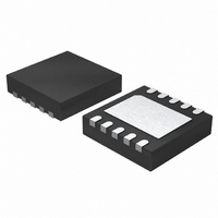
LTC4002EDD-8.4#TR Linear Technology, LTC4002EDD-8.4#TR Datasheet - Page 13

LTC4002EDD-8.4#TR
Manufacturer Part Number
LTC4002EDD-8.4#TR
Description
IC BATT CHARGER SW LI-ION 10DFN
Manufacturer
Linear Technology
Type
Battery Chargerr
Datasheet
1.LTC4002EDD-8.4TR.pdf
(16 pages)
Specifications of LTC4002EDD-8.4#TR
Function
Charge Management
Battery Type
Lithium-Ion (Li-Ion)
Voltage - Supply
8.9 V ~ 22 V
Operating Temperature
-40°C ~ 85°C
Mounting Type
Surface Mount
Package / Case
10-WFDFN Exposed Pad
Output Voltage
8.4V
Operating Supply Voltage (min)
8.9V
Operating Supply Voltage (max)
22V
Operating Temp Range
-40C to 85C
Package Type
DFN
Mounting
Surface Mount
Pin Count
10
Operating Temperature Classification
Industrial
Lead Free Status / RoHS Status
Contains lead / RoHS non-compliant
Lead Free Status / RoHS Status
Contains lead / RoHS non-compliant
Available stocks
Company
Part Number
Manufacturer
Quantity
Price
APPLICATIO S I FOR ATIO
Input and Output Capacitors
Since the input capacitor is assumed to absorb all input
switching ripple current in the converter, it must have an
adequate ripple current rating. Worst-case RMS ripple cur-
rent is approximately one-half of output charge current.
Actual capacitance value is not critical. Solid tantalum
capacitors have a high ripple current rating in a relatively
small surface mount package, but caution must be used
when tantalum capacitors are used for input bypass. High
input surge currents can be created when the adapter is
hot-plugged to the charger and solid tantalum capacitors
have a known failure mechanism when subjected to very
high turn-on surge currents. Selecting the highest pos-
sible voltage rating on the capacitor will minimize prob-
lems. Consult with the manufacturer before use.
The selection of output capacitor C
mined by the ESR required to minimize ripple voltage and
load step transients. The output ripple ∆V
mately bounded by:
Since ∆I
highest at maximum input voltage. Typically, once the ESR
requirement is satisfied, the capacitance is adequate for
filtering and has the necessary RMS current rating.
∆
V
OUT
L
increases with input voltage, the output ripple is
≤ ∆
I ESR
L
⎛
⎜
⎝
U
+
8
U
f
OSC OUT
1
C
W
OUT
⎞
⎟
⎠
is primarily deter-
OUT
is approxi-
U
Switching ripple current splits between the battery and the
output capacitor depending on the ESR of the output ca-
pacitor and the battery impedance. EMI considerations
usually make it desirable to minimize ripple current in the
battery leads. Ferrite beads or an inductor may be added
to increase battery impedance at the 500kHz switching
frequency. If the ESR of the output capacitor is 0.2Ω and
the battery impedance is raised to 4Ω with a bead or induc-
tor, only 5% of the current ripple will flow in the battery.
Design Example
As a design example, take a charger with the following
specifications: V
1.5A, f
First, calculate the SENSE resistor :
Choose the inductor for about 65% ripple current at the
maximum V
Selecting a standard value of 6.8µH results in a maximum
ripple current of :
R
L
∆ =
SENSE
I
=
L
OSC
(
500
(
= 100mV/1.5A = 68mΩ
500
= 500kHz, see Figure 2.
IN
kHz
:
kHz
)(
IN
4
4
0 65 1 5
)
V
V
= 5V to 22V, V
.
(
6 8
.
)(
µ
H
.
)
A
⎛
⎜
⎝
)
1
⎛
⎜
⎝
–
1
22
BAT
–
4
V
22
V
4
= 4V nominal, I
⎞
⎟ =
⎠
V
V
LTC4002
⎞
⎟ =
⎠
962 6
6 713
.
.
mA
13
µ
H
BAT
4002f
=


