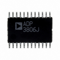
ADP3806JRUZ-REEL7 ON Semiconductor, ADP3806JRUZ-REEL7 Datasheet - Page 6

ADP3806JRUZ-REEL7
Manufacturer Part Number
ADP3806JRUZ-REEL7
Description
IC CHARGER LI-ION ADJ 24-TSSOP
Manufacturer
ON Semiconductor
Datasheet
1.ADP3806JRUZ-REEL7.pdf
(16 pages)
Specifications of ADP3806JRUZ-REEL7
Function
Charge Management
Battery Type
Lithium-Ion (Li-Ion)
Voltage - Supply
13 V ~ 20 V
Operating Temperature
0°C ~ 100°C
Mounting Type
Surface Mount
Package / Case
24-TSSOP
Lead Free Status / RoHS Status
Lead free / RoHS Compliant
Other names
ADP3806JRUZ-REEL7CT
ADP3806
PIN CONFIGURATION AND FUNCTION DESCRIPTIONS
Table 3. Pin Function Descriptions
Pin No.
1
2
3
4
5
6
7
8
9
10
11
12
13
14
15
16
17
18
19
20
21
22
23
24
Mnemonic
VCC
SYS−
SYS+
ISYS
LIMIT
CT
SYNC
REG
REF
SD
COMP
LC
AGND
BAT
BATSEL
ISET
CS−
CS+
PGND
DRVL
BSTREG
BST
DRVH
SW
Function
Supply Voltage.
System Current Sense Output.
System Current Sense Limit Output.
Oscillator Timing Capacitor.
Oscillator Synchronization Pin.
6.0 V Analog Regulator Output.
2.5 V Precision Reference Output.
Shutdown Control Input.
External Compensation Node.
Analog Ground.
Battery Sense Input. 2.5 V for ADP3806. 12.525 V or 16.7 V for ADP3806-12.5. 12.6 V or 16.8 V for ADP3806-12.6.
Battery Voltage Sense Input. High = three cells, low = four cells.
Charge Current Program Input.
Power Ground.
Low Drive Output. This switches between REG and PGND.
7.0 V Regulator Output for Boost.
Floating Bootstrap Supply for DRVH.
High Drive Output. This switches between SW and BST.
Buck Switching Node Reference for DRVH.
Negative System Current Sense Input.
Positive System Current Sense Input.
Low Current Output.
Negative Current Sense Input.
Positive Current Sense Input.
COMP
SYNC
LIMIT
SYS–
SYS+
ISYS
VCC
REG
REF
CT
SD
LC
Figure 2. Pin Configuration
10
11
12
1
2
3
4
5
6
7
8
9
Rev. C | Page 6 of 16
(Not to Scale)
ADP3806
TOP VIEW
24
23
22
21
20
19
18
17
16
15
14
13
ISET
BATSEL
BAT
SW
DRVH
BST
BSTREG
DRVL
PGND
CS+
CS–
AGND


