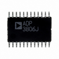
ADP3806JRUZ-REEL7 ON Semiconductor, ADP3806JRUZ-REEL7 Datasheet - Page 11

ADP3806JRUZ-REEL7
Manufacturer Part Number
ADP3806JRUZ-REEL7
Description
IC CHARGER LI-ION ADJ 24-TSSOP
Manufacturer
ON Semiconductor
Datasheet
1.ADP3806JRUZ-REEL7.pdf
(16 pages)
Specifications of ADP3806JRUZ-REEL7
Function
Charge Management
Battery Type
Lithium-Ion (Li-Ion)
Voltage - Supply
13 V ~ 20 V
Operating Temperature
0°C ~ 100°C
Mounting Type
Surface Mount
Package / Case
24-TSSOP
Lead Free Status / RoHS Status
Lead free / RoHS Compliant
Other names
ADP3806JRUZ-REEL7CT
Typical values of R
input range of ISET is from 0 V to 4 V. If, for example, a 3 A
charger is required, R
The power dissipation in R
this example, the power is a maximum of 360 mW. Once R
has been chosen, the charge current can be adjusted during
operation with V
current of 125 mA for trickle charging. The R3, R4, and C13
component s provide high frequency filtering for the current
sense signal.
FINAL BATTERY VOLTAGE CONTROL
As the battery approaches its final voltage, the ADP3806
switches from CC mode to constant voltage (CV) mode. The
change is achieved by the common output node of g
Only one of the two outputs controls the voltage at the COMP
pin. Both amplifiers can only pull down on COMP, such that
when either amplifier has a positive differential input voltage,
its output is not active. For example, when the battery voltage,
V
voltage reaches the desired final voltage, g
loop, and the charge current is reduced.
Amplifier g
reference voltage of 2.5 V. In the case of the ADP3806-12.5 and
ADP3806-12.6, an internal resistor divider sets the selectable
final battery voltage.
When BATSEL is high, the final battery voltage is set to three
cells (12.6 V or 12.525 V). BATSEL can be tied to REG for this
state. When BATSEL is tied to ground, V
(16.8 V or 16.7 V). BATSEL has a 2 μA pull-up current as a fail-
safe to select three cells when it is left open.
BAT
, is low, g
m
2 compares the battery voltage to the internal
m
2 does not control COMP. When the battery
ISET
CS
. Lowering V
range from 25 mΩ to 50 mΩ, and the
CS
could be set to 40 mΩ and V
CS
DRVLSD
should be kept below 500 mW. In
SD
ISET
IN
to 125 mV gives a charge
ADP3806
BOOTSTRAPPED
SYNCHRONOUS DRIVER
1V
BAT
m
2 takes control of the
TIME
–
CMP1
+
OFF
equals four cells
MIN
Figure 20. Bootstrapped Synchronous Driver
m
ISET
1 and g
= 3 V.
CS
DELAY
DELAY
Rev. C | Page 11 of 16
m
2.
CMP3
CMP2
BSTREG
The reference and internal resistor divider are referenced to the
AGND pin, which should be connected close to the negative
terminal of the battery to minimize sensing errors.
In contrast, the ADP3806 requires external, precision resistors.
The divider ratio should be set to divide the desired final
voltage down to 2.5 V at the BAT pin
These resistors should have a parallel impedance of approximately
80 kΩ to minimize bias current errors. When the ADP3806 is in
shutdown, an internal switch disconnects the BAT pin as shown
in Figure 19. This disconnects the resistor (R11) from the
battery and minimizes leakage. The resistance of the internal
switch is less than 200 Ω.
OSCILLATOR AND PWM
The oscillator generates a triangle waveform between 1 V and
2.5 V. This is compared to the voltage at the COMP pin, setting
the duty cycle of the driver stage. When V
duty cycle is zero. Above 2.5 V, the duty cycle reaches its
maximum.
+
–
1V
R11
R12
=
V
ADP3806
BATTERY
2
Figure 19. Battery Sense Disconnect Circuit
5 .
V
g
m
2
+
−
PGND
BST
DRVH
SW
DRVL
CBST
1
BATSEL
V
SD
REF
R12
102kΩ
0.1%
Q1
Q2
BAT
COMP
RR11
412kΩ
0.1%
BATTERY
is below 1 V, the
ADP3806
(2)


