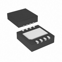
STC3100IQT STMicroelectronics, STC3100IQT Datasheet - Page 12

STC3100IQT
Manufacturer Part Number
STC3100IQT
Description
IC BATTERY MON W/GUAGE 8-DFN
Manufacturer
STMicroelectronics
Type
Battery Monitoringr
Datasheet
1.STC3100IQT.pdf
(21 pages)
Specifications of STC3100IQT
Function
Fuel, Gas Gauge/Monitor
Battery Type
Lithium-Ion (Li-Ion)
Voltage - Supply
2.7 V ~ 5.5 V
Operating Temperature
-40°C ~ 85°C
Mounting Type
Surface Mount
Package / Case
8-DFN
Product
Charge Management
Operating Supply Voltage
2.7 V to 5.5 V
Maximum Operating Temperature
+ 85 C
Minimum Operating Temperature
- 40 C
Mounting Style
SMD/SMT
Temperature Monitoring
Yes
Svhc
No SVHC (15-Dec-2010)
Base Number
3100
Battery Management Function
Monitor
Charge Current Max
2.5A
Control Interface
I2C
Input Voltage Max
5.5V
No. Of Pins
8
Rohs Compliant
Yes
Operating Supply Voltage (min)
2.7V
Operating Supply Voltage (max)
5.5V
Operating Temp Range
-40C to 85C
Mounting
Surface Mount
Pin Count
8
Operating Temperature Classification
Industrial
For Use With
497-10045 - BOARD EVAL BATT MONITOR STC3100
Lead Free Status / RoHS Status
Lead free / RoHS Compliant
Other names
497-8824-2
Available stocks
Company
Part Number
Manufacturer
Quantity
Price
Part Number:
STC3100IQT
Manufacturer:
ST
Quantity:
20 000
I2C interface
8
8.1
Table 6.
Table 7.
Table 8.
12/21
RegADDR7
DATA7
b7
b7
b7
1
I2C interface
Read and write operations
The interface is used to control and read the current accumulator and registers. It is
compatible with the Philips I2C registered trademark (version 2.1). It is a slave serial
interface with a serial data line (SDA) and a serial clock line (SCL).
●
●
A filter rejects the potential spikes on the bus data line to preserve data integrity.
The bidirectional data line supports transfers up to 400 kbit/s (fast mode). The data is shifted
to and from the chip on the SDA line, MSB first.
The first bit must be high (START) followed by the device address and read/write bit control.
Bits DevADDR0 to DevADDR2 are factory-programmable, the default device address value
being 70h (AddrID0 = AddrID1 = AddrID2 = 0). The STC3100 then sends an acknowledge
at the end of an 8-bit long sequence. The next 8 bits correspond to the register address
followed by another acknowledge.
The data field is the last 8-bit long sequence sent, followed by a last acknowledge.
Device address format
Register address format
Register data format
RegADDR6
DATA6
SCL: input clock used to shift data.
SDA: input/output bidirectional data transfers.
b6
b6
b6
1
RegADDR5
DATA5
b5
b5
b5
1
RegADDR4
DATA4
b4
b4
b4
0
DevADDR2
RegADDR3
DATA3
b3
b3
b3
DevADDR1
RegADDR2
DATA2
b2
b2
b2
DevADDR0
RegADDR1
DATA1
b1
b1
b1
RegADDR0
STC3100
DATA0
R/W
b0
b0
b0


