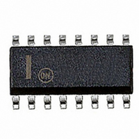
NCP1205DR2G ON Semiconductor, NCP1205DR2G Datasheet - Page 10

NCP1205DR2G
Manufacturer Part Number
NCP1205DR2G
Description
IC CTRLR PWM CM OVP HV 16SOIC
Manufacturer
ON Semiconductor
Datasheet
1.NCP1205DR2.pdf
(17 pages)
Specifications of NCP1205DR2G
Output Isolation
Isolated
Frequency Range
90 ~ 125kHz
Voltage - Input
8 ~ 30 V
Operating Temperature
-25°C ~ 150°C
Package / Case
16-SOIC (0.154", 3.90mm Width)
Number Of Outputs
1
Output Current
250 mA
Mounting Style
SMD/SMT
Switching Frequency
110 KHz
Operating Supply Voltage
30 V
Maximum Operating Temperature
+ 125 C
Fall Time
30 ns
Minimum Operating Temperature
- 25 C
Rise Time
30 ns
Synchronous Pin
No
Topology
Flyback, Forward
Lead Free Status / RoHS Status
Lead free / RoHS Compliant
Other names
NCP1205DR2G
NCP1205DR2GOSTR
NCP1205DR2GOSTR
Available stocks
Company
Part Number
Manufacturer
Quantity
Price
Part Number:
NCP1205DR2G
Manufacturer:
ON/安森美
Quantity:
20 000
In order to clarify the device behavior, we can distinguish the
following simplified operating phases:
Advantages of the Method
NCP1205 brings the following advantages:
By implementing the aforementioned control scheme, the
1. The load is at its nominal value. The SMPS operates in
2. The load starts to decrease and the free- -running
3. The frequency can no longer naturally increase
4. The peak current has reached the internal minimum
5. To further reduce the transmitted power (V
a first order system (at low frequencies) and thus
naturally eases the feedback loop compensation.
smooth turn- -off conditions.
brought by Coss and all the parasitic capacitances.
system into Pulse Duration Modulation. This method
prevents from generating uncontrolled output ripple as
with hysteretic controllers.
the frequency goes down, you ensure that this level is
low enough to avoid transformer acoustic noise
generation even at audible frequencies.
Discontinuous only operation: in DCM, the Flyback is
A low- -cost secondary rectifier can be used due to
Valley switching ensures minimum switching losses
By folding back the switching frequency, you turn the
By letting you control the peak current value at which
borderline conduction mode and the switching
frequency is imposed by the external elements (Vin,
Lp, Ip, Vout). The MOSFET is turned on at the
minimum drain- -source level.
frequency hits the internal clamp.
because of the clamp. The frequency is now controlled
by the internal VCO but remains constant. The peak
current finds no other option that diminishing to satisfy
equation (1).
ceiling level and is now frozen for the remaining
cycles.
the VCO decreases the switching frequency. In case of
output overshoot, the VCO could decrease the
frequency down to zero. When the overshoot has gone,
V
operation.
FB
diminishes again and the IC smoothly resumes its
FB
goes up),
http://onsemi.com
10
Detailed Description
the NCP1205.
Free- -Running Operation
is dictated by the external elements. We can split the different
switching sections in two separated instants. In the following
text we use the internal error voltage, Verr. This level is
elaborated in Figure 13. Verr is linked to VFB (pin 4) by the
following formula:
reach the peak current setpoint imposed by the level on FB
pin (pin 4). Since this level is internally divided by three, the
peak setpoint is simply:
the inductance value and the rectified DC input voltage by:
definition:
transformer depends on the reset voltage applied at the
switch opening. During the conduction time of the
secondary diode, the primary side of the transformer
undergoes a reflected voltage of: [Np/Ns . (Vf + Vout)]. This
voltage applied on the primary inductance dictates the time
needed to decrease from Ip down to zero:
frequency of the SMPS operating in Borderline Conduction
Mode (BCM):
ton + toff =
The following sections describe the internal behavior of
As previously said, the operating frequency at nominal load
ON time: The ON time is given by the time it takes to
The rising slope of the peak current is also dependent on
By combining both equations, we obtain the ON time
OFF time: The time taken by the demagnetization of the
By adding ton + toff, we obtain the natural switching
ton =
· Ip =
3 · Rsense
Verr · Lp
Vin DC
toff =
Ipk =
Lp
Np
Ns
Verr = 10 − 3 · V FB
· (Vout + Vf)
dIL
dt
· Ip =
3 · Rsense
Np
Ns
·
⎪ ⎪
⎪
⎪
=
Vin DC
· (Vout + Vf)
Lp · Verr
1
Vin DC
1
Vin DC · 3 · Rsense
Lp
Lp
Lp · V ERR
+
· 3 · Rsense
· Verr
Np
Ns
· (Vout + Vf)
1
(eq. 2)
(eq. 3)
(eq. 4)
(eq. 5)
(eq. 6)
(eq. 7)
⎤
⎪
⎦


