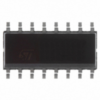
E-L6598D013TR STMicroelectronics, E-L6598D013TR Datasheet - Page 14

E-L6598D013TR
Manufacturer Part Number
E-L6598D013TR
Description
IC CTRLR HV 16SOIC
Manufacturer
STMicroelectronics
Datasheet
1.L6598D013TR.pdf
(24 pages)
Specifications of E-L6598D013TR
Output Isolation
Isolated
Frequency Range
61.8 ~ 400kHz
Voltage - Input
8 ~ 16.6 V
Voltage - Output
600V
Operating Temperature
-40°C ~ 150°C
Package / Case
16-SOIC (0.154", 3.90mm Width)
Output Voltage
4.6 V
Mounting Style
SMD/SMT
Lead Free Status / RoHS Status
Lead free / RoHS Compliant
Other names
497-4588-2
Available stocks
Company
Part Number
Manufacturer
Quantity
Price
Company:
Part Number:
E-L6598D013TR
Manufacturer:
ROHM
Quantity:
2 381
Part Number:
E-L6598D013TR
Manufacturer:
ST
Quantity:
20 000
Block diagram description
5.4
14/24
The bootstrap driver introduces a voltage drop during the recharging of the capacitor Cboot
(i.e. when the low side driver is on), which increases with the frequency and with the size of
the external power MOS. It is the sum of the drop across the R
threshold voltage. At low frequency this drop is very small and can be neglected. Anyway
increasing the frequency it must be taken in to account. In fact the drop, reducing the
amplitude of the driving signal, can significantly increase the R
MOS (and so the dissipation).
To be considered that in resonant power supplies the current which flows in the power MOS
decreases increasing the switching frequency and generally the increases of R
problem because power dissipation is negligible. The following equation is useful to
compute the drop on the bootstrap driver:
Equation 8
where Q
bootstrap DMOS, and T
semi-period of the switching frequency minus the dead time). The typical resistance value of
the bootstrap DMOS is 150 Ω. For example using a power MOS with a total gate charge of
30 nC the drop on the bootstrap driver is about 3 V, at a switching frequency of 200 kHz. In
fact:
Equation 9
To summaries, if a significant drop on the bootstrap driver (at high switching frequency when
large power MOS are used) represents a problem, an external diode can be used, avoiding
the drop on the R
Op amp section
The integrated op amp is designed to offer low output impedance, wide band, high input
impedance and wide common mode range. It can be readily used to implement protection
features or a closed loop control. For this purpose the op amp output can be properly
connected to R
g
is the gate charge of the external power MOS, R
fmin
V
DSON
drop
pin to adjust the oscillation frequency.
=
of the DMOS.
charge
I
ch
arg
V
e
is the time in which the bootstrap driver remains on (about the
R
drop
Doc ID 6554 Rev 7
dson
=
+
------------------ 150Ω
2.23μs
V
30nC
diode
→
V
drop
+
0.6V 2.6V
=
------------------ - R
T
∼
ch
Q
arg
dson
g
e
DSON
DSON
is the on resistance of the
dson
+
of the external power
and of the diode
V
diode
DSON
is not a
L6598


