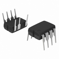
NCP1028P065G ON Semiconductor, NCP1028P065G Datasheet - Page 20

NCP1028P065G
Manufacturer Part Number
NCP1028P065G
Description
IC SWIT HV 8DIP
Manufacturer
ON Semiconductor
Datasheet
1.NCP1028P065G.pdf
(29 pages)
Specifications of NCP1028P065G
Output Isolation
Isolated
Frequency Range
58.5 ~ 71.5kHz
Voltage - Input
7.2 ~ 10 V
Voltage - Output
700V
Power (watts)
25W
Operating Temperature
0°C ~ 150°C
Package / Case
8-DIP (0.300", 7.62mm), 7 Leads
Lead Free Status / RoHS Status
Lead free / RoHS Compliant
Available stocks
Company
Part Number
Manufacturer
Quantity
Price
Part Number:
NCP1028P065G
Manufacturer:
ON/安森美
Quantity:
20 000
Over Power Compensation
represents a way to limit the effects of the propagation
delay when the converter is supplied from its highest input
voltage. The propagation delay naturally extends the
power capability of any current-limited converter.
Figure 35 explains why. The main parameter is the on
slope, that is to say, the pace at which the inductor current
grows-up when the power switch closes. For a flyback
controller, the slope is given by:
where
inductance and
Over Power Compensation or Protection (OPP)
that it is difficult to keep an adequate level on the
Figure 34. The burst frequency becomes so low
amount of time before shutting off the driving
Figure 35. Internal logic blocks take a certain
pulses in presence of an overcurrent event.
L
p
is the transformer magnetizing/primary
V
in
> 30 ms
, the input voltage.
auxiliary V
S on +
V in
L p
CC
.
http://onsemi.com
(eq. 4)
NCP1028
20
gate shutdown does not immediately occur when the
maximum power limit is detected (just before activating
the overload protection circuit). Clearly speaking, it can
take up to 100 ns for the NCP1028 current sense
comparator to propagate through the various logical gates
before reaching the power switch and finally shutting it off.
This is the well-known propagation delay noted
Unfortunately, during this time, the current keeps growing
as Figure 35 depicts. The peak current will therefore be
troubled by this propagation delay. The formula to obtain
the final value is simply:
final peak value. The situation differs at high line and
induces a higher peak current. Therefore, the power supply
output power capability increases with the input voltage.
Let us a take a look at a simple example. Suppose the peak
current is 700 mA:
L
V
V
I
t
Where:
Usually h is bigger in high line conditions than in low line
conditions. This formula is valid for a Discontinuous
Conduction Mode flyback.
in both conditions:
I
I
output power capability again, in both conditions with
respective low and high line efficiency numbers of 78%
and 82% for instance:
P
P
prop
peak,max
peak,final
peak,final
out,lowline
out,highline
p
in
in
As the internal logic takes some time to react, the switch
At low line,
From Equation 5, we can calculate the final peak current
From Equation 6, we can have an idea of the maximum
= 1.0 mH
lowline = 100 Vdc
highline = 350 Vdc
= 100 ns
F
= 700 mA
sw
= (100/1m) x 100n + 700m = 710 mA at low line.
= (350/1m) x 100n + 700m = 735 mA at high line.
I peak, final +
= 0.5
= 0.5
is the switching frequency and h the efficiency.
P out + 1
S
on
is relatively low and does not bother the
0.71
0.735
2
I 2 peak, final F SW L p h
V in
2
L p
2
t
prop
1m
1m
) I peak, max
65k
65k
0.78 = 12.8 W
0.82 = 14.4 W
(eq. 5)
(eq. 6)
t
prop
.


