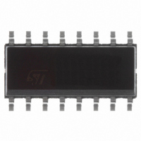
L6668 STMicroelectronics, L6668 Datasheet - Page 3

L6668
Manufacturer Part Number
L6668
Description
IC CTRLR PWM PROG CM HV 16SOIC
Manufacturer
STMicroelectronics
Datasheet
1.L6668TR.pdf
(23 pages)
Specifications of L6668
Output Isolation
Isolated
Frequency Range
93 ~ 107kHz
Voltage - Input
9.4 ~ 22 V
Power (watts)
750mW
Operating Temperature
-25°C ~ 150°C
Package / Case
16-SOIC (0.154", 3.90mm Width)
Number Of Outputs
1
Duty Cycle (max)
75 %
Output Current
800 mA
Mounting Style
SMD/SMT
Switching Frequency
105 KHz
Maximum Operating Temperature
+ 150 C
Fall Time
30 ns
Minimum Operating Temperature
- 25 C
Rise Time
55 ns
Synchronous Pin
No
Topology
Flyback
Load-dependent Current-mode Control
FIXED-FREQUENCY (HEAVY LOAD), FREQUENCY FOLDBACK (LIGHT LOAD), BURST-MODE (NO-LOAD)
For Use With
497-6389 - BOARD EVAL USING L6668 & STSR30497-5499 - EVAL BOARD FOR L6668
Lead Free Status / RoHS Status
Lead free / RoHS Compliant
Available stocks
Company
Part Number
Manufacturer
Quantity
Price
Company:
Part Number:
L6668TR
Manufacturer:
TOSHIBA
Quantity:
19 162
Part Number:
L6668TR
Manufacturer:
ST
Quantity:
20 000
Part Number:
L6668TR-1LF
Manufacturer:
ST
Quantity:
20 000
Table 4. Pin Description
Number
Pin
10
11
12
1
2
3
4
5
6
7
8
9
Pin Name
SKIPADJ
COMP
VREF
ISEN
GND
HVS
OUT
N.C.
Vcc
DIS
HV
SS
High-voltage start-up. The pin is to be connected directly to the rectified mains voltage. A
0.8 mA internal current source charges the capacitor connected between pin Vcc and GND
to start up the IC. When the voltage on the Vcc pin reaches the start-up threshold the gen-
erator is shut down. Normally it is re-enabled when the voltage on the Vcc pin falls below
5V, except under latched shutdown conditions, when it is re-enabled as the Vcc voltage falls
0.5V below the start-up threshold.
High-voltage spacer. The pin is not connected internally to isolate the high-voltage pin and
comply with safety regulations (creepage distance) on the PCB.
Chip ground. Current return for both the gate-drive current and the bias current of the IC. All
of the ground connections of the bias components should be tied to a track going to this pin
and kept separate from any pulsed current return.
Gate-drive output. The driver is capable of 0.8A min. source/sink peak current to drive
MOSFET’s. The voltage delivered to the gate is clamped at about 15V so as to prevent too
high values when the IC is supplied with a voltage close to or exceeding 20V.
Supply Voltage of both the signal part of the IC and the gate driver. The internal high volt-
age generator charges an electrolytic capacitor connected between this pin and GND as
long as the voltage on the pin is below the start-up threshold of the IC, after that it is dis-
abled. Sometimes a small bypass capacitor (0.1µF typ.) to GND might be useful to get a
clean bias voltage for the signal part of the IC.
Connect the pin to GND.
Latched device shutdown. Internally the pin connects a comparator that, when the voltage
on the pin exceeds 2.2V, shuts the IC down and brings its consumption to a value barely
higher than before start-up. The information is latched and it is necessary to recycle the
input power to restart the IC: the latch is removed as the voltage on the Vcc pin goes below
the UVLO threshold. Connect the pin to GND if the function is not used.
Voltage reference. An internal generator furnishes an accurate voltage reference (5V±4%,
all inclusive) that can be used to supply up to 5 mA to an external circuit. A small film
capacitor (0.1µF typ.), connected between this pin and GND is recommended to ensure the
stability of the generator and to prevent noise from affecting the reference.
Burst-mode control threshold. A voltage is applied to this pin, derived from the reference
voltage VREF via a resistor divider. When the control voltage at pin COMP falls 50 mV
below the voltage on this pin the IC is shutdown and the consumption is reduced. The chip
is re-enabled as the voltage on pin COMP exceeds the voltage on the pin. The high-voltage
start-up generator is not invoked. The function is disabled during the soft-start ramp. The
pin must always be biased between 0.8 and 2.5V. A voltage between 0.8 and 1.4V disables
the function, if the pin is pulled below 0.8V the IC is shut down.
Control input for PWM regulation. The pin is to be driven by the phototransistor (emitter-
grounded) of an optocoupler to modulate the voltage by modulating the current sunk from
(sourced by) the pin (0.4 mA typ.). It is recommended to place a small filter capacitor
between the pin and GND, as close to the IC as possible to reduce switching noise pick up,
to set a pole in the output-to-control transfer function. A voltage 50 mV lower than that on
pin SKIPADJ shuts down the IC and reduces its current consumption.
Soft start. An internal 20µA generator charges an external capacitor connected between
the pin and GND generating a voltage ramp across it. This ramp clamps the voltage at pin
COMP during start-up, thus the duty cycle of the power switch starts from zero. During the
ramp all functions monitoring the voltage at pin COMP are disabled. The SS capacitor is
quickly discharged as the chip goes into UVLO.
Current sense (PWM comparator) input. The voltage on this pin is internally compared with
an internal reference derived from the voltage on pin COMP and when they are equal the
gate drive output (previously asserted high by the clock signal generated by the oscillator)
is driven low to turn off the power MOSFET. The pin is equipped with 200 ns. min. blanking
time for improved noise immunity. A second comparison level located at 1.5V shuts the
device down and brings its consumption almost to a “before start-up” level.
Function
L6668
3/23


