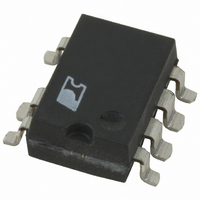
LNK354GN Power Integrations, LNK354GN Datasheet - Page 4

LNK354GN
Manufacturer Part Number
LNK354GN
Description
IC OFFLINE SWIT OCP HV 8SMD
Manufacturer
Power Integrations
Series
LinkSwitch®-HFr
Type
Off Line Switcherr
Datasheet
1.LNK353GN-TL.pdf
(16 pages)
Specifications of LNK354GN
Output Isolation
Isolated
Frequency Range
186 ~ 214kHz
Voltage - Output
700V
Power (watts)
5W
Operating Temperature
-40°C ~ 150°C
Package / Case
8-SMD Gull Wing, 7 Leads
Output Voltage
5.8 V
Input / Supply Voltage (max)
265 VAC
Input / Supply Voltage (min)
85 VAC
Duty Cycle (max)
63 %
Switching Frequency
200 KHz
Supply Current
280 uA
Operating Temperature Range
- 40 C to + 150 C
Mounting Style
SMD/SMT
Lead Free Status / RoHS Status
Lead free / RoHS Compliant
Available stocks
Company
Part Number
Manufacturer
Quantity
Price
Company:
Part Number:
LNK354GN
Manufacturer:
POWER
Quantity:
15 000
Figure 5. Universal Input, 5.7 V, 400 mA, Constant Voltage, Constant Current Battery Charger Using LinkSwitch-HF.
Applications Example
A 2.4 W CC/CV Charger Adapter
The circuit shown in Figure 5 is a typical implementation of
a 5.7 V, 400 mA, constant voltage, constant current (CV/CC)
battery charger.
The input bridge formed by diodes D1-D4, rectifies the AC
input voltage. The rectified AC is then filtered by the bulk
storage capacitors C1 and C2. Resistor RF1 is a flameproof,
fusible, wire wound type and functions as a fuse, inrush current
limiter and, together with the π filter formed by C1, C2 and L1,
differential mode noise attenuator.
This simple EMI filtering, together with the frequency jittering
of LinkSwitch-HF (U1), a small value Y1 capacitor (CY1),
and shield windings within T1, and a secondary-side RC
snubber (R5, C5), allows the design to meet both conducted
and radiated EMI limits. The low value of CY1 is important
to meet the requirement of low line frequency leakage current,
in this case <10 µA.
The rectified and filtered input voltage is applied to the primary
winding of T1. The other side of the transformer primary is
driven by the integrated MOSFET in U1. Diode D5, C3, R1
and R3 form the primary clamp network. This limits the peak
drain voltage due to leakage inductance. Resistor R3 allows the
use of a slow, low cost rectifier diode by limiting the reverse
current through D5 when U1 turns on. The selection of a slow
diode improves efficiency and conducted EMI.
85-265
4
VAC
J1
J2
LNK353/354
2.5 W
8.2 Ω
RF1
F
2/05
1N4005
1N4005
D1
D3
1N4005
1N4005
4.7 µF
D2
400 V
D4
C1
1 mH
L1
100 kΩ
4.7 µF
400 V
R1
C2
LinkSwitch-HF
LNK354P
2.2 nF
400 V
200 Ω
U1
C3
R3
1N4007GP
D5
5
3
4 5
NC NC
Output rectification is provided by Schottky diode D6. The low
forward voltage provides high efficiency across the operating
range and the low ESR capacitor C6 minimizes output voltage
ripple.
In constant voltage (CV) mode, the output voltage is set by the
Zener diode VR1 and the emitter-base voltage of PNP transistor
Q1. The V
current through VR1 (~2.7 mA). When the output voltage
exceeds the threshold voltage determined by Q1 and VR1, Q1
is turned on and current flows through the LED of U2. As the
LED current increases, the current fed into the FEEDBACK
pin increases, disabling further switching cycles of U1. At
very light loads, almost all switching cycles will be disabled,
giving a low effective switching frequency and providing low
no-load consumption.
During load transients, R6 and R8 ensure that the ratings of Q1 are
not exceeded while R4 prevents C4 from being discharged.
Resistors R9 and R10 form the constant current (CC) sense
circuit. Above approximately 400 mA, the voltage across the
sense resistor exceeds the optocoupler diode forward conduction
voltage of approximately 1 V. The current through the LED
is therefore determined by the output current and CC control
dominates over the CV feedback loop. CC control is maintained
even under output short circuit conditions.
100 pF
CY1
EE16
T1
100 nF
5.1 kΩ
9
8
C4
R4
BE
of Q1 divided by the value of R7 sets the bias
2.2 nF
68 Ω
R5
C5
PC817D
SS14
D6
U2B
PC817D
330 µF
16 V
U2A
390 Ω
C6
MMST
3906
R8
Q1
6.8 Ω
200 Ω
2.4 Ω
R10
1 W
R6
R9
PI-3891-070204
220 Ω
BZX79B5V1
5.1 V, 2%
R7
VR1
400 mA
5.7 V,
J3-2
RTN
J3-1


