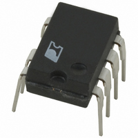
TNY268PN Power Integrations, TNY268PN Datasheet - Page 10

TNY268PN
Manufacturer Part Number
TNY268PN
Description
IC OFFLINE SWIT OTP OCP HV 8DIP
Manufacturer
Power Integrations
Series
TinySwitch®-IIr
Specifications of TNY268PN
Output Isolation
Isolated
Frequency Range
124 ~ 140kHz
Voltage - Output
700V
Power (watts)
23W
Operating Temperature
-40°C ~ 150°C
Package / Case
8-DIP (0.300", 7.62mm), 7 Leads
Output Voltage
5.8 V
Input / Supply Voltage (max)
265 VAC
Input / Supply Voltage (min)
85 VAC
Duty Cycle (max)
68 %
Switching Frequency
132 KHz
Supply Current
380 uA
Operating Temperature Range
- 40 C to + 150 C
Mounting Style
Through Hole
Supply Voltage
265VAC
Digital Ic Case Style
DIP
No. Of Pins
8
No. Of Regulated Outputs
1
Filter Terminals
DIP
Rohs Compliant
Yes
On Resistance Rds(on)
5.2ohm
Lead Free Status / RoHS Status
Lead free / RoHS Compliant
Other names
596-1055-5
Available stocks
Company
Part Number
Manufacturer
Quantity
Price
Company:
Part Number:
TNY268PN
Manufacturer:
PowerInt
Quantity:
260 650
Company:
Part Number:
TNY268PN
Manufacturer:
POWER
Quantity:
20 000
Part Number:
TNY268PN
Manufacturer:
POWER
Quantity:
20 000
*Not available.
Key Application Considerations
TinySwitch-II vs. TinySwitch
Table 2 compares the features and performance differences
between the TNY254 device of the TinySwitch-II family with
the TinySwitch-II family of devices. Many of the new features
eliminate the need for or reduce the cost of circuit components.
Other features simplify the design and enhance performance.
Design
Output Power
Table 1 (front page) shows the practical continuous output
power levels that can be obtained under the following
conditions:
Table 2.
TinySwitch-II vs. TinySwitch
Switching Frequency and
Tolerance
Temperature Variation
(0-100 °C)**
Active Frequency Jitter
Transformer Audible Noise
Reduction
Line UV Detect
Current Limit Tolerance
Temperature Variation
(0-100 °C)**
Auto-Restart
BYPASS Pin Zener Clamp
DRAIN Creepage at Package
Rev. H 02/09
Function
10
Comparison Between TinySwitch and TinySwitch-II.
TNY263-268
** See typical performance curves.
44 kHz ±10% (at 25 °C)
+8%
N/A*
N/A*
N/A*
±11% (at 25 °C)
-8%
N/A*
N/A*
0.037 in. / 0.94 mm
TinySwitch
TNY254
132 kHz ±6% (at 25 °C)
+2%)
±4 kHz
Yes–built into controller
Single resistor
programmable
±7% (at 25 °C)
0%)
6% effective on-time
Internally clamped to 6.3 V
0.137 in. / 3.48 mm
TinySwitch-II
TNY263-268
1.
2.
3.
4.
In addition to the thermal environment (sealed enclosure,
ventilated, open frame, etc.), the maximum power capability of
TinySwitch-II in a given application depends on transformer
The minimum DC input voltage is 90 V or higher for
85 VAC input, or 240 V or higher for 230 VAC input or
115 VAC input with a voltage doubler. This corresponds to
a fi lter capacitor of 3 μF/W for universal input and 1 μF/W
for 230 VAC or 115 VAC with doubler input.
A secondary output of 5 V with a Schottky rectifi er diode.
Assumed effi ciency of 77% (TNY267 & TNY268), 75%
(TNY265 & TNY266) and 73% (TNY263 & TNY264).
The parts are board mounted with SOURCE pins soldered
to suffi cient area of copper to keep the die temperature at
or below 100 °C.
•
•
•
•
•
•
•
•
•
•
•
•
•
•
Smaller transformer for low cost
Ease of design
Manufacturability
Optimum design for lower cost
Lower EMI minimizing fi lter
component costs
Practically eliminates audible noise with ordinary dip
varnished transformer – no special
construction or gluing required
Prevents power on/off glitches
Increases power capability and
simplifi es design for high volume
manufacturing
Limits output short-circuit current to less than full
load current
Protects load in open loop fault conditions
Allows TinySwitch-II to be powered from a low
voltage bias winding to improve effi ciency and to
reduce on-chip power dissipation
Greater immunity to arcing as a result of dust,
debris or other contaminants build-up
No output diode size penalty
No additional components required
TinySwitch-II
Advantages
www.powerint.com


