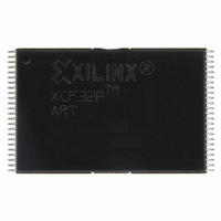
XCF32PVOG48C Xilinx Inc, XCF32PVOG48C Datasheet - Page 34

XCF32PVOG48C
Manufacturer Part Number
XCF32PVOG48C
Description
IC PROM SRL 1.8V 32M GATE 48TSOP
Manufacturer
Xilinx Inc
Datasheet
1.XCF01SVOG20C.pdf
(35 pages)
Specifications of XCF32PVOG48C
Programmable Type
In System Programmable
Memory Size
32Mb
Voltage - Supply
1.65 V ~ 2 V
Operating Temperature
-40°C ~ 85°C
Package / Case
48-TFSOP (0.472", 12.0mm Width)
Lead Free Status / RoHS Status
Lead free / RoHS Compliant
Other names
122-1458
122-1458-5
122-1458-5
122-1458-5
122-1458-5
Available stocks
Company
Part Number
Manufacturer
Quantity
Price
Company:
Part Number:
XCF32PVOG48C
Manufacturer:
XILINX
Quantity:
1 200
Company:
Part Number:
XCF32PVOG48C
Manufacturer:
XILINX
Quantity:
308
Company:
Part Number:
XCF32PVOG48C
Manufacturer:
XILINX/41
Quantity:
974
Part Number:
XCF32PVOG48C
Manufacturer:
XILINX/赛灵思
Quantity:
20 000
DS123 (v2.18) May 19, 2010
Product Specification
12/29/05
05/09/06
12/08/06
02/01/07
03/30/07
01/28/08
03/31/08
04/03/08
05/14/08
07/07/08
11/14/08
10/26/09
(Cont’d)
Date
R
Version
2.11.1
2.13.1
2.10
2.11
2.12
2.13
2.14
2.15
2.16
2.17
2.8
2.9
• Notes for
• Enhanced description under section
• Enhanced description on design revision sampling under section
• Figure 4 and Figure 5 renamed to
• Value for
• Block diagram in
• Added Virtex-5 LX support to Table 2.
•
• Added Virtex-5 LXT support to Table 2.
• Defined reprogramming operation requirements in
• Corrected statements regarding the FPGA BUSY pin and corrected various references.
• Removed Spartan-3L support and added Spartan-3A and Virtex-5 SXT support to Table 2.
• Corrected Spartan-3E bitstream sizes in Table 2.
• Correct supported voltages for
Added Spartan-3A DSP support to Table 2.
• Added support for XC5VLX155, XC5VLX20T, and XC5VLX155T.
• Updated JTAG TAP timing specifications in
• Tied FPGA CS_B and FPGA RDWR_B to GND in the FPGA SelectMAP schematics to ensure
• Hardwired external oscillator to FPGA CCLK in the FPGA slave mode schematics.
• Added marking templates
• Other edits and updates made.
• Updated document template.
• Updated URLs.
• Added Virtex-5 FX FPGA support to Table 2.
• Corrected markings for all packaging
• Added note regarding variances in packaging and marking to
• Corrected typo.
• Updated trademark notations.
Added support for XC5VSX240T and Platform Flash XL to Table 2.
Updated
Added Virtex-5 TXT FPGA to Table 2.
• Globally changed PROG_B and PROGRAM to PROGRAM_B.
• Removed the following information from this data sheet to UG161, Platform Flash PROM User
• Moved “up to 33 MHz” from FPGA Configuration Interface bullets in
•
• Added statement about ignoring non-JTAG input pins to second paragraph of
• Added reference to Platform Flash PROM User Guide in
page
need for a pull-up resistor if CF is not connected to PROGB.
figures, and table and figure references renumber this point forward.
functional blocks.
"VIL"
to match LVCMOS25 standard.
page
valid logic Low.
for 48-pin TFBGA packages in
Guide:
• Table 2 entitled “Xilinx FPGAs and Compatible Platform Flash PROMs”
• Section entitled “PROM to FPGA Configuration Mode and Connections Summary”
• Section entitled “Configuration PROM-to-FPGA Device Interface Connection Diagrams”
"Description," page
Table 1, page
from 1.5V to 1.8V. Added table note 1 about design revisioning for the XCF08P.
Programming," page
"Internal Oscillator," page
20,
maximum for 2.5V operation in
26.
"Write Protection," page
Figure 11, page
Figure 6, page
"ICCINT," page 15
1: Changed lower bound on V
Figure 2, page 2
1, and added reference to related considerations.
www.xilinx.com
Platform Flash In-System Programmable Configuration PROMs
3.
16,
21,
8.
(Figure 14, page
Figure 7, page
updated from 5mA to 1mA for XCFxxP.
Figure 12, page
4.
"Marking Information," page
"VCCJ"
updated to show clock source muxing and route clocking to all
Table 7, page 8
"CLKOUT," page
"Recommended Operating Conditions," page 14
(Figure 14, page
in
Revision
Table 12, page
17,
Table 9, page 7
31,
CCO
22, and
Figure 8, page
Figure 15
for XCF08P, XCF16P, and XCF32P devices
and
"Programming," page
Figure 13, page 23
8.
31,
Table 8, page 8
"External Programming," page 3
24,
and
Figure
to reflect improved performance.
30.
"VCCO"
Page
18,
Figure
"Design Revisioning," page
15, and
Figure 9, page
31.
"Features," page 1
16), and corrected marks
and
respectively. All tables,
3.
updated to specify the
Figure
"VCCJ"
"In-System
19,
16).
in
Figure 10,
Table 13,
updated
to
and
8.
34


