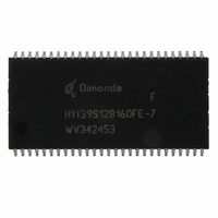
HYI39S128160FE-7 Qimonda, HYI39S128160FE-7 Datasheet - Page 16

HYI39S128160FE-7
Manufacturer Part Number
HYI39S128160FE-7
Description
IC SDRAM 128MBIT 143MHZ 54TSOP
Manufacturer
Qimonda
Datasheet
1.HYI39S128800FE-7.pdf
(21 pages)
Specifications of HYI39S128160FE-7
Format - Memory
RAM
Memory Type
SDRAM
Memory Size
128M (8Mx16)
Speed
143MHz
Interface
Parallel
Voltage - Supply
3 V ~ 3.6 V
Operating Temperature
-40°C ~ 85°C
Package / Case
54-TSOP II
Lead Free Status / RoHS Status
Lead free / RoHS Compliant
Other names
675-1019-2
1)
2) For proper power-up see the operation section of this data sheet.
3) AC timing tests for LV-TTL versions have
4) If clock rising time is longer than 1 ns, a time (t
5) Access time from clock
6) If
7) These parameter account for the number of clock cycles and depend on the operating frequency of the clock, as follows:the number of
8) It is recommended to use two clock cycles between the last data-in and the precharge command in case of a write command without Auto-
9) When a Write command with Auto Precharge has been issued, a time of
Rev. 1.32, 2007-10
10122006-I6LJ-WV3H
Parameter
Write Cycle
Last Data Input to Precharge
(Write without Auto Precharge)
Last Data Input to Activate(Write with Auto Precharge)
DQM Write Mask Latency
T
time is measured between
Specified
rate between 0.8 V and 2.0 V.
components with no termination and 0 pF load.
clock cycles = specified value of timing period (counted in fractions as a whole number)
Precharge. One clock cycle between the last data-in and the precharge command is also supported, but restricted to cycle times
or equal the specified
be applied. For each of the terms, if not already an integer, round up to the next highest integer.
A
t
T
= 0 to 70 °C;
is longer than 1 ns, a time (
t
AC
CLOCK
INPUT
OUTPUT
and
V
t
t
SS
IS
OH
= 0 V;
1.4 V
parameters are measured with a 50 pF only, without any resistive termination and with an input signal of 1V / ns edge
t
WR value, where
t
ac
is 4.6 ns for PC133 components with no termination and 0 pF load,Data out hold time
t
t
V
V
LZ
IH
IH
DD
t
AC
,
and
t
T
V
DDQ
- 1) ns has to be added to this parameter.
1.4 V
V
t
CL
IL
= 3.3 V ± 0.3 V,
. All AC measurements assume
t
V
ck
IL
is equal to the actual system clock time.
t
t
OH
= 0.4 V and
CH
t
T
T
t
t
AC
/2 - 0.5) ns has to be added to this parameter.
HZ
2.4 V
0.4 V
IO.vsd
t
T
V
= 1 ns
1.4 V
IH
= 2.4 V with the timing referenced to the 1.4 V crossover point. The transition
16
t
T
Symbol
t
t
t
= 1 ns with the AC output load circuit shown in figure below.
t
WR
DAL(min.)
DQW
DAL(min)
Measurement conditions for
I/O
has be fullfilled before the next Activate Command can
t
Measurement conditions for
AC
Min.
14
0
and
HY[B/I]39S128[40/80/16][0/7]F[E/T](L)
t
50 pF
PC133– 222
OH
t
CK
–7
Max.
—
—
is equal to the actual system clock time.
128-MBit Synchronous DRAM
ns
t
t
CK
CK
Unit
t
oh
is 1.8 ns for PC133
FIGURE 2
Note
1)2)3)8)
1)2)3)9)
1)2)3)
t
Data Sheet
AC
t
and
CK
greater
t
OH


