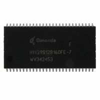
HYI39S128160FE-7 Qimonda, HYI39S128160FE-7 Datasheet

HYI39S128160FE-7
Specifications of HYI39S128160FE-7
Related parts for HYI39S128160FE-7
HYI39S128160FE-7 Summary of contents
Page 1
...
Page 2
... IDD for low power option 0 “Transition time” replaced by “Transition Time of Clock (Rise and Fall)” 4 Added HYI39S128800FT-7, HYI39S128800FE-7, HYI39S128160FT-7, HYI39S128160FE-7 and HYB39S128407FE-7 Previous Revision: 2006-10, Rev. 1.20 We Listen to Your Comments Any information within this document that you feel is wrong, unclear or missing at all? Your feedback will help us to continuously improve the quality of this document ...
Page 3
... The chip is fabricated with Qimonda’s advanced 0.11 μm 128-MBit DRAM process technology. The device is designed to comply with all industry standards set for synchronous DRAM products, both electrically and mechanically ...
Page 4
... Industrial Operating Temperature (- °C) HYI39S128800FE-7 PC133–222–520 HYI39S128160FE-7 1) RoHS Compliant Product: Restriction of the use of certain hazardous substances (RoHS) in electrical and electronic equipment as defined in the directive 2002/95/EC issued by the European Parliament and of the Council of 27 January 2003. These substances include mercury, lead, cadmium, hexavalent chromium, polybrominated biphenyls and polybrominated biphenyl ethers ...
Page 5
Chip Configuration This chapter contains the pin configuration table, the TSOP package drawing, and the block diagrams for the ×4, ×8, ×16 organization of the SDRAM. 2.1 Pin Description Listed below are the pin configurations sections for the various ...
Page 6
Ball No. Name Pin Buffer Type Type Data Signals ×4 Organization 5 DQ0 I/O LVTTL 11 DQ1 I/O LVTTL 44 DQ2 I/O LVTTL 50 DQ3 I/O LVTTL Data Signals ×8 Organization 2 DQ0 I/O LVTTL 5 DQ1 I/O LVTTL 8 ...
Page 7
Ball No. Name Pin Buffer Type Type Power Supplies ×4/×8/×16 Organization V 9 PWR – DDQ V 14 PWR – PWR – SSQ V 41 PWR – SS Not connected ×4 Organization ...
Page 8
Package P(G)–TSOPII–54 Listed below are the pin outs of the TSOP package. Rev. 1.32, 2007-10 10122006-I6LJ-WV3H HY[B/I]39S128[40/80/16][0/7]F[E/T](L) 128-MBit Synchronous DRAM Pin Configuration P(G)-TSOPII-54 8 Data Sheet FIGURE 1 ...
Page 9
Functional Description This chapter list all defined commands and their usage for this Synchronous DRAM family. Operation Device State 3) Bank Active Idle Bank Precharge Any Precharge All Any 3) Write Active 3) Write with Auto Active precharge 3) ...
Page 10
Field Bits Type BL 2 6:4 TM 8:7 WBL 9 12:10 Rev. 1.32, 2007-10 10122006-I6LJ-WV3H Mode Register Definition (BA Description Burst Length Number of sequential bits per DQ related to one read/write command Note: All other ...
Page 11
Burst Length Starting Column Address FullPage n Notes 1. For a burst length of two, ...
Page 12
Electrical Characteristics 4.1 Operating Conditions Parameter V Input / Output voltage relative Voltage on supply relative Voltage on supply relative to DDQ SS Operating Temperature for HYB... Operating Temperature for ...
Page 13
Parameter Supply Voltage I/O Supply Voltage Input high voltage Input low voltage I Output high voltage ( = – 4.0 mA) OUT I Output low voltage ( = 4.0 mA) OUT V Input leakage current, any input(0 V < Output ...
Page 14
Parameter Operating Current One bank active, Burst length = 1 Precharge Standby Current in Power Down Mode Recharge Standby Current in Non-Power Down Mode No Operating Current Active state (max. 4 banks) Burst Operating Current Read command cycling Auto Refresh ...
Page 15
AC Characteristics Parameter Clock and Clock Enable Clock Frequency Access Time from Clock Clock High Pulse Width Clock Low Pulse Width Transition Time of Clock (Rise and Fall) Setup and Hold Times Input Setup Time Input Hold Time CKE ...
Page 16
Parameter Write Cycle Last Data Input to Precharge (Write without Auto Precharge) Last Data Input to Activate(Write with Auto Precharge) DQM Write Mask Latency ° 3.3 ...
Page 17
Package Outlines Notes 1. Drawing according to ISO 8015 2. Dimensions General tolerances +/- 0.15 Rev. 1.32, 2007-10 10122006-I6LJ-WV3H HY[B/I]39S128[40/80/16][0/7]F[E/T](L) 128-MBit Synchronous DRAM Package Outline PG-TSOPII-54-4 (top view) 17 Data Sheet FIGURE 3 ...
Page 18
List of Figures Figure 1 Pin Configuration P(G)-TSOPII- ...
Page 19
List of Tables Table 1 Performance . . . . . . . . . . . . . . . . . . . . . . . . . . . . . . . . . . ...
Page 20
Table of Contents 1 Overview . . . . . . . . . . . . . . . . . . . . . . . . . . . . . . . . . . . ...
Page 21
... Due to technical requirements components may contain dangerous substances. For information on the types in question please contact your nearest Qimonda Office. Qimonda Components may only be used in life-support devices or systems with the express written approval of Qimonda failure of such components can reasonably be expected to cause the failure of that life-support device or system affect the safety or effectiveness of that device or system ...


