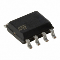
M24512-WMN6P STMicroelectronics, M24512-WMN6P Datasheet - Page 25

M24512-WMN6P
Manufacturer Part Number
M24512-WMN6P
Description
IC EEPROM 512KBIT 400KHZ 8SOIC
Manufacturer
STMicroelectronics
Specifications of M24512-WMN6P
Format - Memory
EEPROMs - Serial
Memory Type
EEPROM
Memory Size
512K (64K x 8)
Speed
400kHz
Interface
I²C, 2-Wire Serial
Voltage - Supply
2.5 V ~ 5.5 V
Operating Temperature
-40°C ~ 85°C
Package / Case
8-SOIC (3.9mm Width)
Memory Configuration
64K X 8
Interface Type
I2C, Serial
Clock Frequency
1MHz
Access Time
500ns
Supply Voltage Range
2.5V To 5.5 V
Memory Case Style
SOIC
No. Of Pins
8
Rohs Compliant
Yes
Lead Free Status / RoHS Status
Lead free / RoHS Compliant
Other names
497-8582-5
M24512-WMN6P
M24512-WMN6P
Available stocks
Company
Part Number
Manufacturer
Quantity
Price
Company:
Part Number:
M24512-WMN6P
Manufacturer:
PANASONIC
Quantity:
60 000
Part Number:
M24512-WMN6P
Manufacturer:
ST
Quantity:
20 000
M24512-R, M24512-W, M24512-DR
Table 11.
1. Sampled only, not 100% tested.
2. E2,E1,E0: Input impedance when the memory is selected (after a Start condition).
Table 12.
1. The new M24512-W devices (identified by the process letter K) offer I
2. Characterized value, not tested in production.
3. The device is not selected after power-up, after a Read instruction (after the Stop condition), or after the
Symbol
Symbol
I
I
V
V
Z
I
I
Z
CC0
CC1
V
completion of the internal write cycle t
I
CC
C
C
LO
OL
LI
H
L
IH
IL
IN
IN
(2)
(2)
Input leakage current
(SCL, SDA, E0, E1,
E2)
Output leakage
current
Supply current (Read)
Supply current (Write)
Standby supply
current
Input low voltage
(SCL, SDA, WC)
Input high voltage
(SCL, SDA)
Input high voltage
(WC, E0, E1, E2)
Output low voltage
Input capacitance (SDA)
Input capacitance (other pins)
Input impedance
(E2, E1, E0, WC)
Input impedance
(E2, E1, E0, WC)
Input parameters
DC characteristics (voltage range W)
Parameter
Parameter
(1)
Doc ID 16459 Rev 22
V
device in Standby mode
SDA in Hi-Z, external voltage applied
on SDA: V
V
(rise/fall time < 50 ns)
V
(rise/fall time < 50 ns)
2.5 V < V
(rise/fall time < 50 ns)
During t
Device not selected
V
= 2.5 V
V
I
I
OL
OL
IN
CC
CC
IN
IN
Test conditions (see
W
= 2.1 mA, V
= 3 mA, V
= V
= V
= V
= 2.5 V, f
= 5.5 V, f
(t
W
SS
SS
SS
W
is triggered by the correct decoding of a Write instruction).
CC
, 2.5 V < V
or V
or V
or V
SS
< 5.5 V, f
c
c
or V
CC
CC
CC
CC
Test condition
Table
= 400 kHz
= 400 kHz
V
V
CC
, V
, V
= 5.5 V
IN
IN
CC
= 2.5 V or
(3)
CC
< 0.3V
> 0.7V
CC
CC
10)
c
,
= 5.5 V
= 1 MHz
< 5.5 V
Device grade 3
Device grade 6
Table 8
CC
CC
CC
and
= 1.5 mA.
Min.
500
30
DC and AC parameters
0.7V
0.7V
–0.45
Min.
CC
CC
Max.
8
6
V
0.3V
CC
Max.
1
5
± 2
± 2
2.5
6.5
0.4
2
5
2
3
(1)
(2)
+0.6
CC
Unit
k
k
pF
pF
Unit
25/41
mA
mA
mA
mA
µA
µA
µA
µA
V
V
V


