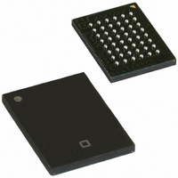
CY62157DV30L-55BVXET Cypress Semiconductor Corp, CY62157DV30L-55BVXET Datasheet - Page 5

CY62157DV30L-55BVXET
Manufacturer Part Number
CY62157DV30L-55BVXET
Description
IC SRAM 8MBIT 55NS 48VFBGA
Manufacturer
Cypress Semiconductor Corp
Datasheet
1.CY62157DV30LL-55ZSXI.pdf
(12 pages)
Specifications of CY62157DV30L-55BVXET
Format - Memory
RAM
Memory Type
SRAM
Memory Size
8M (512K x 16)
Speed
55ns
Interface
Parallel
Voltage - Supply
2.2 V ~ 3.6 V
Operating Temperature
-40°C ~ 125°C
Package / Case
48-VFBGA
Lead Free Status / RoHS Status
Lead free / RoHS Compliant
Available stocks
Company
Part Number
Manufacturer
Quantity
Price
Company:
Part Number:
CY62157DV30L-55BVXET
Manufacturer:
Cypress Semiconductor Corp
Quantity:
10 000
Document #: 38-05392 Rev. *H
Switching Characteristics
Read Cycle
t
t
t
t
t
t
t
t
t
t
t
t
t
t
Write Cycle
t
t
t
t
t
t
t
t
t
t
t
Notes:
15. BHE.BLE is the AND of both BHE and BLE. Chip can be deselected by either disabling the chip enable signals or by disabling both BHE and BLE.
16. Test conditions for all parameters other than tri-state parameters assume signal transition time of 3 ns or less, timing reference levels of V
17. At any given temperature and voltage condition, t
18. t
19. The internal Write time of the memory is defined by the overlap of WE, CE
RC
AA
OHA
ACE
DOE
LZOE
HZOE
LZCE
HZCE
PU
PD
DBE
LZBE
HZBE
WC
SCE
AW
HA
SA
PWE
BW
SD
HD
HZWE
LZWE
Parameter
levels of 0 to V
given device.
a write and any of these signals can terminate a write by going INACTIVE. The data input set-up and hold timing should be referenced to the edge of the signal
that terminates the write.
HZOE
, t
HZCE
, t
[19]
HZBE
CC(typ.)
Read Cycle Time
Address to Data Valid
Data Hold from Address Change
CE
OE LOW to Data Valid
OE LOW to LOW Z
OE HIGH to High Z
CE
CE
CE
CE
BLE/BHE LOW to Data Valid
BLE/BHE LOW to Low Z
BLE/BHE HIGH to HIGH Z
Write Cycle Time
CE
Address Set-up to Write End
Address Hold from Write End
Address Set-up to Write Start
WE Pulse Width
BLE/BHE LOW to Write End
Data Set-up to Write End
Data Hold from Write End
WE LOW to High-Z
WE HIGH to Low-Z
, and t
1
1
1
1
1
1
, and output loading of the specified I
HZWE
LOW and CE
LOW and CE
HIGH and CE
LOW and CE
HIGH and CE
LOW and CE
transitions are measured when the outputs enter a high-impedance state.
Description
Over the Operating Range
2
2
2
2
2
2
[17]
[17, 18]
[17, 18]
[17]
HIGH to Data Valid
HIGH to Low Z
HIGH to Power-Up
HIGH to Write End
LOW to High Z
LOW to Power-Down
HZCE
[17]
[17, 18]
is less than t
OL
/I
[17]
OH
[17, 18]
as shown in the “AC Test Loads and Waveforms” section.
LZCE
, t
HZBE
1
[16]
= V
Min.
45
10
10
10
45
40
40
35
40
25
10
5
0
0
0
0
IL
is less than t
45 ns
, BHE and/or BLE = V
[13]
Max.
45
45
25
15
20
45
45
15
15
LZBE
, t
HZOE
Min.
55
10
10
10
55
40
40
40
40
25
10
IL
5
0
0
0
0
is less than t
, and CE
55 ns
CY62157DV30 MoBL
2
Max.
= V
55
55
25
20
20
55
55
20
20
LZOE
IH
. All signals must be ACTIVE to initiate
, and t
Min.
HZWE
70
10
10
10
70
60
60
45
60
30
10
5
0
0
0
0
70 ns
is less than t
CC(typ)
Max.
70
70
35
25
25
70
70
25
25
Page 5 of 12
/2, input pulse
LZWE
Unit
for any
ns
ns
ns
ns
ns
ns
ns
ns
ns
ns
ns
ns
ns
ns
ns
ns
ns
ns
ns
ns
ns
ns
ns
ns
ns
®
[+] Feedback


