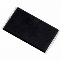
NAND02GW3B2AN6F STMicroelectronics, NAND02GW3B2AN6F Datasheet - Page 29

NAND02GW3B2AN6F
Manufacturer Part Number
NAND02GW3B2AN6F
Description
IC FLASH 2GBIT 48TSOP
Manufacturer
STMicroelectronics
Datasheet
1.NAND01GW3A0AN6E.pdf
(64 pages)
Specifications of NAND02GW3B2AN6F
Format - Memory
FLASH
Memory Type
FLASH - Nand
Memory Size
2G (256M x 8)
Interface
Parallel
Voltage - Supply
2.7 V ~ 3.6 V
Operating Temperature
-40°C ~ 85°C
Package / Case
48-TSOP
Lead Free Status / RoHS Status
Lead free / RoHS Compliant
Speed
-
NAND01G-B, NAND02G-B
6.4
Copy Back Program
The Copy Back Program operation is used to copy the data stored in one page and
reprogram it in another page.
The Copy Back Program operation does not require external memory and so the operation
is faster and more efficient because the reading and loading cycles are not required. The
operation is particularly useful when a portion of a block is updated and the rest of the block
needs to be copied to the newly assigned block.
If the Copy Back Program operation fails an error is signalled in the Status Register.
However as the standard external ECC cannot be used with the Copy Back Program
operation bit error due to charge loss cannot be detected. For this reason it is recommended
to limit the number of Copy Back Program operations on the same data and or to improve
the performance of the ECC.
The Copy Back Program operation requires four steps:
1.
2.
3.
To see the Data Input cycle for modifying the source page and an example of the Copy Back
Program operation refer to
A data input cycle to modify a portion or a multiple distant portion of the source page, is
shown in
Table 11.
1. DD = Dual Die
Table 12.
1. DD = Dual Die
1 Gbit
2 Gbit
2 Gbit DD
1 Gbit
2 Gbit
2 Gbit DD
The first step reads the source page. The operation copies all 1056 Words/ 2112 Bytes
from the page into the Data Buffer. It requires:
–
–
–
When the device returns to the ready state (Ready/Busy High), the next bus write cycle
of the command is given with the 4 bus cycles to input the target page address. Refer
to
Then the confirm command is issued to start the P/E/R Controller.
Table 11
Figure 13
one bus write cycle to setup the command
4 bus write cycles to input the source page address
one bus write cycle to issue the confirm command code
(1)
(1)
Density
Density
Copy Back Program x8 Addresses
Copy Back Program x16 Addresses
for the addresses that must be the same for the Source and Target pages.
Figure
12.
Same Address for Source and Target Pages
Same Address for Source and Target Pages
no constraint
no constraint
no constraint
no constraint
A28
A27
Device operations
29/64


