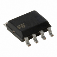
M93S46-WMN6P STMicroelectronics, M93S46-WMN6P Datasheet - Page 4

M93S46-WMN6P
Manufacturer Part Number
M93S46-WMN6P
Description
IC EEPROM 1KBIT 2MHZ 8SOIC
Manufacturer
STMicroelectronics
Datasheet
1.M93S46-WMN6TP.pdf
(34 pages)
Specifications of M93S46-WMN6P
Format - Memory
EEPROMs - Serial
Memory Type
EEPROM
Memory Size
1K (64 x 16)
Speed
2MHz
Interface
Microwire, 3-Wire Serial
Voltage - Supply
2.5 V ~ 5.5 V
Operating Temperature
-40°C ~ 85°C
Package / Case
8-SOIC (3.9mm Width)
Organization
64 K x 16
Interface Type
Microwire
Maximum Clock Frequency
2 MHz
Supply Voltage (max)
5.5 V
Supply Voltage (min)
2.5 V
Maximum Operating Current
2 mA
Maximum Operating Temperature
+ 85 C
Mounting Style
SMD/SMT
Minimum Operating Temperature
- 40 C
Operating Supply Voltage
2.5 V, 5.5 V
Memory Configuration
64 X 16
Clock Frequency
2MHz
Supply Voltage Range
2.5V To 5.5V
Memory Case Style
SOIC
No. Of Pins
8
Rohs Compliant
Yes
Lead Free Status / RoHS Status
Lead free / RoHS Compliant
Other names
497-8596-5
M93S46-WMN6P
M93S46-WMN6P
Available stocks
Company
Part Number
Manufacturer
Quantity
Price
Company:
Part Number:
M93S46-WMN6P
Manufacturer:
STMicroelectronics
Quantity:
1 958
Company:
Part Number:
M93S46-WMN6P
Manufacturer:
ST
Quantity:
6 390
Part Number:
M93S46-WMN6P
Manufacturer:
ST
Quantity:
20 000
M93S66, M93S56, M93S46
SUMMARY DESCRIPTION
This specification covers a range of 4K, 2K, 1K bit
serial Electrically Erasable Programmable Memo-
ry (EEPROM) products (respectively for M93S66,
M93S56, M93S46). In this text, these products are
collectively referred to as M93Sx6.
Figure 2. Logic Diagram
Table 1. Signal Names
The M93Sx6 is accessed through a serial input (D)
and output (Q) using the MICROWIRE bus proto-
col. The memory is divided into 256, 128, 64 x16
bit words (respectively for M93S66, M93S56,
M93S46).
The M93Sx6 is accessed by a set of instructions
which includes Read, Write, Page Write, Write All
4/34
S
D
Q
C
PRE
W
V
V
CC
SS
PRE
W
D
C
S
V CC
V SS
Chip Select Input
Serial Data Input
Serial Data Output
Serial Clock
Protection Register Enable
Write Enable
Supply Voltage
Ground
M93Sx6
Q
AI02020
and instructions used to set the memory protec-
tion. These are summarized in
3.).
A Read Data from Memory (READ) instruction
loads the address of the first word to be read into
an internal address pointer. The data contained at
this address is then clocked out serially. The ad-
dress pointer is automatically incremented after
the data is output and, if the Chip Select Input (S)
is held High, the M93Sx6 can output a sequential
stream of data words. In this way, the memory can
be read as a data stream from 16 to 4096 bits (for
the M93S66), or continuously as the address
counter automatically rolls over to 00h when the
highest address is reached.
Within the time required by a programming cycle
(t
Page Write instruction. the whole memory may
also be erased, or set to a predetermined pattern,
by using the Write All instruction.
Within the memory, a user defined area may be
protected against further Write instructions. The
size of this area is defined by the content of a Pro-
tection Register, located outside of the memory ar-
ray. As a final protection step, data may be
permanently protected by programming a One
Time Programming bit (OTP bit) which locks the
Protection Register content.
Programming is internally self-timed (the external
clock signal on Serial Clock (C) may be stopped or
left running after the start of a Write cycle) and
does not require an erase cycle prior to the Write
instruction. The Write instruction writes 16 bits at a
time into one of the word locations of the M93Sx6,
the Page Write instruction writes up to 4 words of
16 bits to sequential locations, assuming in both
cases that all addresses are outside the Write Pro-
tected area. After the start of the programming cy-
cle, a Busy/Ready signal is available on Serial
Data Output (Q) when Chip Select Input (S) is driv-
en High.
Figure 3. DIP, SO and TSSOP Connections
Note: See
W
), up to 4 words may be written with help of the
sions, and how to identify pin-1.
PACKAGE MECHANICAL
Q
C
D
S
1
2
3
4
M93Sx6
AI02021
8
7
6
5
section for package dimen-
Table 2.
V CC
PRE
W
V SS
and
Table


