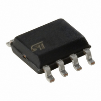
M24C01-WMN6P STMicroelectronics, M24C01-WMN6P Datasheet - Page 9

M24C01-WMN6P
Manufacturer Part Number
M24C01-WMN6P
Description
IC EEPROM 1KBIT 400KHZ 8SOIC
Manufacturer
STMicroelectronics
Datasheets
1.M24C01-WMN6TP.pdf
(39 pages)
2.M24C04-WMN6P.pdf
(29 pages)
3.M24C01-WMN6P.pdf
(40 pages)
Specifications of M24C01-WMN6P
Format - Memory
EEPROMs - Serial
Memory Type
EEPROM
Memory Size
1K (128 x 8)
Speed
400kHz
Interface
I²C, 2-Wire Serial
Voltage - Supply
2.5 V ~ 5.5 V
Operating Temperature
-40°C ~ 85°C
Package / Case
8-SOIC (3.9mm Width)
Organization
128 K x 8
Interface Type
I2C
Maximum Clock Frequency
0.4 MHz
Access Time
900 ns
Supply Voltage (max)
5.5 V
Supply Voltage (min)
2.5 V
Maximum Operating Current
2 mA
Maximum Operating Temperature
+ 85 C
Mounting Style
SMD/SMT
Minimum Operating Temperature
- 40 C
Operating Supply Voltage
2.5 V, 5.5 V
Memory Configuration
128 X 8
Clock Frequency
400kHz
Supply Voltage Range
2.5V To 5.5V
Memory Case Style
SOIC
No. Of Pins
8
Rohs Compliant
Yes
Density
1Kb
Access Time (max)
900ns
Frequency (max)
400KHz
Write Protection
Yes
Data Retention
40Year
Operating Supply Voltage (typ)
3.3/5V
Package Type
SOIC
Operating Temp Range
-40C to 85C
Supply Current
2mA
Operating Supply Voltage (min)
2.5V
Operating Supply Voltage (max)
5.5V
Operating Temperature Classification
Industrial
Mounting
Surface Mount
Pin Count
8
Lead Free Status / RoHS Status
Lead free / RoHS Compliant
Other names
497-8558
M24C01-WMN6P
M24C01-WMN6P
Available stocks
Company
Part Number
Manufacturer
Quantity
Price
M24C16, M24C08, M24C04, M24C02, M24C01
2.4
2.4.1
2.4.2
2.4.3
2.4.4
Supply voltage (V
Operating supply voltage V
Prior to selecting the memory and issuing instructions to it, a valid and stable V
within the specified [V
Table
V
V
This voltage must remain stable and valid until the end of the transmission of the instruction
and, for a Write instruction, until the completion of the internal write cycle (t
Power-up conditions
The V
defined in
Device reset
In order to prevent inadvertent write operations during power-up, a power-on-reset (POR)
circuit is included. At power-up (continuous rise of V
instruction until V
than the minimum V
V
mode. The device, however, must not be accessed until V
voltage within the specified [V
In a similar way, during power-down (continuous decrease in V
below the power-on-reset threshold voltage, the device stops responding to any instruction
sent to it.
Power-down conditions
During power-down (continuous decrease in V
mode (mode reached after decoding a Stop condition, assuming that there is no internal
write cycle in progress).
Figure 5.
CC
CC
CC
/V
line with a suitable capacitor (usually of the order of 10 nF to 100 nF) close to the
passes over the POR threshold, the device is reset and enters the Standby Power
8). In order to secure a stable DC supply voltage, it is recommended to decouple the
CC
SS
100
10
4 k
voltage has to rise continuously from 0 V up to the minimum V
package pins.
1
Table
10
Here R bus × C bus = 120 ns
Maximum R
6,
CC
Table 7
30 pF
CC
reaches the power-on-reset threshold voltage (this threshold is lower
CC
Bus line capacitor (pF)
operating voltage defined in
(min), V
P
CC
and
value versus bus parasitic capacitance (C) for an I²C bus
100
CC
)
Doc ID 5067 Rev 16
Table 8
CC
(min), V
CC
(max)] range must be applied (see
and the rise time must not vary faster than 1 V/µs.
CC
(max)] range.
1000
CC
), the device must be in the Standby Power
When t
f
time constant must be below the
400 ns time constant line
represented on the left.
C
= 400 kHz), the R bus × C bus
CC
Table
LOW
), the device does not respond to any
= 1.3 µs (min value for
CC
6,
Table 7
reaches a valid and stable V
CC
), as soon as V
I²C bus
master
and
Table
CC
Signal description
Table
SCL
SDA
operating voltage
W
6,
).
V
CC
8). When
Table 7
CC
R
C
CC
bus
bus
voltage
drops
M24xxx
ai14796b
and
9/39
CC


