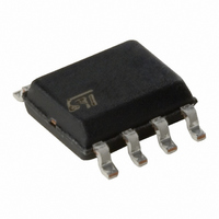
M24C01-WMN6P STMicroelectronics, M24C01-WMN6P Datasheet - Page 13

M24C01-WMN6P
Manufacturer Part Number
M24C01-WMN6P
Description
IC EEPROM 1KBIT 400KHZ 8SOIC
Manufacturer
STMicroelectronics
Datasheets
1.M24C01-WMN6TP.pdf
(39 pages)
2.M24C04-WMN6P.pdf
(29 pages)
3.M24C01-WMN6P.pdf
(40 pages)
Specifications of M24C01-WMN6P
Format - Memory
EEPROMs - Serial
Memory Type
EEPROM
Memory Size
1K (128 x 8)
Speed
400kHz
Interface
I²C, 2-Wire Serial
Voltage - Supply
2.5 V ~ 5.5 V
Operating Temperature
-40°C ~ 85°C
Package / Case
8-SOIC (3.9mm Width)
Organization
128 K x 8
Interface Type
I2C
Maximum Clock Frequency
0.4 MHz
Access Time
900 ns
Supply Voltage (max)
5.5 V
Supply Voltage (min)
2.5 V
Maximum Operating Current
2 mA
Maximum Operating Temperature
+ 85 C
Mounting Style
SMD/SMT
Minimum Operating Temperature
- 40 C
Operating Supply Voltage
2.5 V, 5.5 V
Memory Configuration
128 X 8
Clock Frequency
400kHz
Supply Voltage Range
2.5V To 5.5V
Memory Case Style
SOIC
No. Of Pins
8
Rohs Compliant
Yes
Density
1Kb
Access Time (max)
900ns
Frequency (max)
400KHz
Write Protection
Yes
Data Retention
40Year
Operating Supply Voltage (typ)
3.3/5V
Package Type
SOIC
Operating Temp Range
-40C to 85C
Supply Current
2mA
Operating Supply Voltage (min)
2.5V
Operating Supply Voltage (max)
5.5V
Operating Temperature Classification
Industrial
Mounting
Surface Mount
Pin Count
8
Lead Free Status / RoHS Status
Lead free / RoHS Compliant
Other names
497-8558
M24C01-WMN6P
M24C01-WMN6P
Available stocks
Company
Part Number
Manufacturer
Quantity
Price
M24C16, M24C08, M24C04, M24C02, M24C01
3.6
3.6.1
Figure 7.
Write operations
Following a Start condition the bus master sends a device select code with the Read/Write
bit (RW) reset to 0. The device acknowledges this, as shown in
address byte. The device responds to the address byte with an acknowledge bit, and then
waits for the data byte.
When the bus master generates a Stop condition immediately after a data byte’s Ack bit (in
the “10
cycle is triggered. A Stop condition at any other time slot does not trigger the internal write
cycle.
During the internal Write cycle, Serial Data (SDA) and Serial Clock (SCL) are ignored, and
the device does not respond to any requests.
Byte Write
After the device select code and the address byte, the bus master sends one data byte. If
the addressed location is Write-protected, by Write Control (WC) being driven High (during
the period from the Start condition until the end of the address byte), the device replies to
the data byte with NoAck, as shown in
WC
Byte Write
WC
Page Write
WC (cont'd)
Page Write
(cont'd)
th
bit” time slot), either at the end of a Byte Write or a Page Write, the internal write
Write mode sequences with WC = 1 (data write inhibited)
NO ACK
Dev select
Dev select
Data in N
Doc ID 5067 Rev 16
R/W
R/W
ACK
ACK
NO ACK
Byte address
Byte address
Figure
7, and the location is not modified. If, instead,
ACK
ACK
Data in 1
Data in
NO ACK
NO ACK
Figure
Data in 2
8, and waits for an
NO ACK
Device operation
Data in 3
AI02803d
13/39


