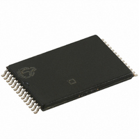
CY7C199CN-20ZXI Cypress Semiconductor Corp, CY7C199CN-20ZXI Datasheet

CY7C199CN-20ZXI
Specifications of CY7C199CN-20ZXI
Related parts for CY7C199CN-20ZXI
CY7C199CN-20ZXI Summary of contents
Page 1
... The device features an automatic power consumption when deselected. See the “Truth Table” on page 3 complete description of read and write modes. The CY7C199CN is available in Pb-free 28-pin TSOP I, 28-pin Molded SOJ and 28-pin DIP package(s). Input Buffer RAM Array Power Column Decoder Down Circuit – ...
Page 2
... Pin Layout and Specifications 28 DIP Document #: 001-06435 Rev TSOP 13.4 mm CY7C199CN 28 SOJ Page ...
Page 3
... WE IOx X High-Z H Data Out L Data In H High-Z Description 0°C to 70°C –40°C to 85°C CY7C199CN SOJ TSOP 10, 11, 12, 13, 14, 15, 16, 17 18, 19, 20, 22, 23, 24, 25, 18 Mode Power Deselect/Power Down Stand by (I Read Active (I Write ...
Page 4
... ≥ ≥ V ≤ max , CE ≥ V – 0.3V ≥ V ≤ 0.3V – 0.3V Output Disabled CC CC CY7C199CN –12 –15 Min Max Min Max – 2 0 – –0.5 0.8 –0.5 0.8 – 2.4 – 2.4 – – – 0.4 – ...
Page 5
... Tested initially and after any design or process change that may affect these parameters. Document #: 001-06435 Rev. *B Conditions T = 25° MHz 5. Conditions TSOP I Still air, soldered × 4.5 square inch, two–layer printed circuit board jig ita Description CY7C199CN Max 8 8 SOJ DIP 88.6 79 69.33 21.94 41.42 31. & ...
Page 6
... V – 0.3V ≥ V ≤ 0.3V V – 0. less than less than t HZCE LZCE HZOE LZOE “” on page 1. Transitions are measured ± 200 mV from steady state voltage. CY7C199CN –20 –25 Min Max Min Max – 20 – – 20 – – 3 – – ...
Page 7
... WE is HIGH for read cycle. 11. This cycle is OE controlled and WE is HIGH read cycle. 12. Address valid before or similar with CE transition LOW. Document #: 001-06435 Rev. *B DATA RETENTION MODE OHA ACE t DOE t LZOE t LZCE t PU 50% CY7C199CN t R Data Valid t HZCE t HZOE High Z Data Valid t PD 50% Page ...
Page 8
... During this period the IOs are in output state and input signals must not be applied. 16. This cycle is CE controlled. 17 goes HIGH simultaneously with WE going HIGH, the output remains in a high impedance state. Document #: 001-06435 Rev SCE PWE t SD Data-In Valid SCE Data-In Valid . IH CY7C199CN High Z Page ...
Page 9
... Write Cycle 3 (WE controlled, OE low) Address Data Undefined In Out see footnotes Note 18. The cycle is WE controlled, OE LOW. The minimum write cycle time is the sum of t Document #: 001-06435 Rev. *B [18 SCE PWE t HZWE and t HZWE SD CY7C199CN Undefined Data In Valid See Footnotes t LZWE . Page ...
Page 10
... CY7C199CN–15VXC 51-85031 CY7C199CN–15ZC 51-85071 CY7C199CN–15ZXC 51-85071 CY7C199CN–15VI 51-85031 CY7C199CNL–15VC 51-85031 CY7C199CNL–15VXC 51-85031 CY7C199CNL–15ZXC 51-85071 CY7C199CNL–15VXI 51-85031 20 CY7C199CN–20VC 51-85031 CY7C199CN–20ZI 51-85071 CY7C199CN–20ZXI 51-85071 25 CY7C199CN–25PC 51-85014 CY7C199CN–25PXC 51-85014 Document #: 001-06435 Rev. *B ...
Page 11
... Package Diagrams Document #: 001-06435 Rev. *B Figure 1. 28-pin TSOP 13.4 mm), 51-85071 CY7C199CN 51-85071-*G Page ...
Page 12
... TYP. Document #: 001-06435 Rev. *B Figure 2. 28-pin (300 Mil) Molded SOJ, 51-85031 PIN 0.291 0.330 0.300 0.350 28 SEATING PLANE 0.120 0.140 0.004 0.025 MIN. CY7C199CN A DETAIL EXTERNAL LEAD DESIGN 0.026 0.032 0.013 0.014 0.019 0.020 OPTION 1 OPTION 2 0.007 0.013 0.262 51-85031-*C ...
Page 13
... SEATING PLANE 1.345[34.16] 1.385[35.18] 0.120[3.05] 0.140[3.55] 0.015[0.38] 0.060[1.52] 0.055[1.39] 0.065[1.65] 0.015[0.38] 0.020[0.50] SEE LEAD END OPTION CY7C199CN DIMENSIONS IN INCHES [MM] MIN. MAX. REFERENCE JEDEC MO-095 PACKAGE WEIGHT: 2.15 gms 0.290[7.36] 0.325[8.25] 0.009[0.23] 3° MIN. 0.012[0.30] 0.310[7.87] 0.385[9.78] 51-85014-*D Page ...
Page 14
... Document History Page Document Title: CY7C199CN, 256K (32K x 8) Static RAM Document Number: 001-06435 Issue REV. ECN No. Date ** 430363 See ECN *A 684342 See ECN *B 839904 See ECN Document #: 001-06435 Rev. *B Orig. of Description of Change Change NXR New Data Sheet VKN Added Automotive-A Information ...


