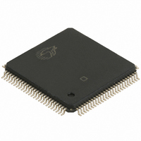
CY7C024-25AXC Cypress Semiconductor Corp, CY7C024-25AXC Datasheet - Page 8

CY7C024-25AXC
Manufacturer Part Number
CY7C024-25AXC
Description
IC SRAM 64KBIT 25NS 100LQFP
Manufacturer
Cypress Semiconductor Corp
Type
Asynchronousr
Datasheet
1.CY7C024-55AXC.pdf
(21 pages)
Specifications of CY7C024-25AXC
Memory Size
64K (4K x 16)
Package / Case
100-LQFP
Format - Memory
RAM
Memory Type
SRAM - Dual Port, Asynchronous
Speed
25ns
Interface
Parallel
Voltage - Supply
4.5 V ~ 5.5 V
Operating Temperature
0°C ~ 70°C
Access Time
25 ns
Supply Voltage (max)
5.5 V
Supply Voltage (min)
4.5 V
Maximum Operating Current
250 mA
Maximum Operating Temperature
+ 70 C
Minimum Operating Temperature
0 C
Mounting Style
SMD/SMT
Number Of Ports
2
Operating Supply Voltage
5 V
Lead Free Status / RoHS Status
Lead free / RoHS Compliant
Lead Free Status / RoHS Status
Lead free / RoHS Compliant, Lead free / RoHS Compliant
Other names
428-2089
CY7C024-25AXC
CY7C024-25AXC
Available stocks
Company
Part Number
Manufacturer
Quantity
Price
Company:
Part Number:
CY7C024-25AXC
Manufacturer:
CY
Quantity:
29
Company:
Part Number:
CY7C024-25AXC
Manufacturer:
Cypress Semiconductor Corp
Quantity:
10 000
Company:
Part Number:
CY7C024-25AXCT
Manufacturer:
Cypress Semiconductor Corp
Quantity:
10 000
Electrical Characteristics
Capacitance
Document #: 38-06035 Rev. *D
OUTPUT
I
I
I
I
I
C
C
CC
SB1
SB2
SB3
SB4
Parameter
OUTPUT
Note
IN
OUT
13. Tested initially and after any design or process changes that may affect these parameters.
C = 30 pF
(a) Normal Load (Load 1)
Parameter
Load (Load 2)
Operating Current
Standby Current
(Both Ports TTL Levels)
Standby Current
(One Port TTL Level)
Standby Current
(Both Ports CMOS
Levels)
Standby Current
(Both Ports CMOS
Levels)
[13]
C = 30 pF
Description
5V
R1 = 893Ω
R2 = 347Ω
Input Capacitance
Output Capacitance
Over the Operating Range (continued)
Description
GND
3.0V
V
Outputs Disabled
CE
f = f
CE
f = f
Both Ports CE and CE
V
or V
One Port CE
CE
V
Active Port Outputs, f = f
CC
IN
Figure 3. AC Test Loads and Waveforms
CC
R
L
L
≥ V
≤
MAX
MAX
IN
– 0.2V, V
= Max, I
and CE
or CE
≥ V
OUTPUT
3 ns
≤ 0.2V, f = 0
(b) Thévenin Equivalent (Load 1)
CC
10%
[12]
[12]
CC
– 0.2V or V
C = 30pF
Test Conditions
R
– 0.2V,
R
≥ V
IN
L
OUT
ALL INPUT PULSES
or
≥ V
≥ V
IH
90%
[12]
= 0 mA,
IH
,
T
V
CC
A
CC
,
IN
= 25
R
– 0.2V
R
MAX
≤ 0.2V,
= 5.0V
TH
≥
×
= 250Ω
[12]
Test Conditions
C, f = 1 MHz,
Com’l
Ind
Com’l
Ind
Com’l
Ind
Com’l
Ind
Com’l
Ind
90%
V
TH
10%
= 1.4V
7C024/024A/0241–35
≤
Min
3 ns
7C025/0251–35
OUTPUT
Typ
160
160
30
30
85
85
80
80
3
3
(c) Three-State Delay (Load 3)
C = 5 pF
Max
230
260
135
150
120
135
50
65
15
15
CY7C024/024A/0241
Max
10
10
7C024/024A/0241–55
Min
7C025/0251–55
CY7C025/0251
5V
Typ
150
150
20
20
75
75
70
70
3
3
R1 = 893Ω
R2 = 347Ω
Unit
pF
pF
Page 8 of 21
Max
230
260
135
150
120
135
50
65
15
15
Unit
mA
mA
mA
mA
mA
[+] Feedback


