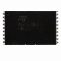
M29F200BB70N6T NUMONYX, M29F200BB70N6T Datasheet - Page 17

M29F200BB70N6T
Manufacturer Part Number
M29F200BB70N6T
Description
IC FLASH 2MBIT 70NS 48TSOP
Manufacturer
NUMONYX
Datasheet
1.M29F200BB70N6T.pdf
(39 pages)
Specifications of M29F200BB70N6T
Format - Memory
FLASH
Memory Type
FLASH - Nor
Memory Size
2M (256K x 8 or 128K x 16)
Speed
70ns
Interface
Parallel
Voltage - Supply
4.5 V ~ 5.5 V
Operating Temperature
-40°C ~ 85°C
Package / Case
48-TSOP
Lead Free Status / RoHS Status
Contains lead / RoHS non-compliant
Other names
497-1707-2
Available stocks
Company
Part Number
Manufacturer
Quantity
Price
Company:
Part Number:
M29F200BB70N6T
Manufacturer:
ST
Quantity:
5 530
Company:
Part Number:
M29F200BB70N6T
Manufacturer:
ST
Quantity:
5 530
Company:
Part Number:
M29F200BB70N6T
Manufacturer:
ST
Quantity:
5 530
M29F200BT, M29F200BB
4.0.4
4.0.5
4.0.6
4.0.7
After the program operation has completed the memory will return to the Read mode, unless
an error has occurred. When an error occurs the memory will continue to output the Status
Register. A Read/Reset command must be issued to reset the error condition and return to
Read mode.
Note that the Program command cannot change a bit set at ’0’ back to ’1’. One of the Erase
Commands must be used to set all the bits in a block or in the whole memory from ’0’ to ’1’.
Unlock Bypass command
The Unlock Bypass command is used in conjunction with the Unlock Bypass Program
command to program the memory. When the access time to the device is long (as with
some EPROM programmers) considerable time saving can be made by using these
commands. Three Bus Write operations are required to issue the Unlock Bypass command.
Once the Unlock Bypass command has been issued the memory will only accept the Unlock
Bypass Program command and the Unlock Bypass Reset command. The memory can be
read as if in Read mode.
Unlock Bypass Program command
The Unlock Bypass Program command can be used to program one address in memory at
a time. The command requires two Bus Write operations, the final write operation latches
the address and data in the internal state machine and starts the Program/Erase Controller.
The Program operation using the Unlock Bypass Program command behaves identically to
the Program operation using the Program command. A protected block cannot be
programmed; the operation cannot be aborted and the Status Register is read. Errors must
be reset using the Read/Reset command, which leaves the device in Unlock Bypass Mode.
See the Program command for details on the behavior.
Unlock Bypass Reset command
The Unlock Bypass Reset command can be used to return to Read/Reset mode from
Unlock Bypass Mode. Two Bus Write operations are required to issue the Unlock Bypass
Reset command.
Chip Erase command
The Chip Erase command can be used to erase the entire chip. Six Bus Write operations
are required to issue the Chip Erase Command and start the Program/Erase Controller.
If any blocks are protected then these are ignored and all the other blocks are erased. If all
of the blocks are protected the Chip Erase operation appears to start but will terminate
within about 100µs, leaving the data unchanged. No error condition is given when protected
blocks are ignored.
During the erase operation the memory will ignore all commands. It is not possible to issue
any command to abort the operation. Typical chip erase times are given in
Read operations during the Chip Erase operation will output the Status Register on the Data
Inputs/Outputs. See the section on the Status Register for more details.
After the Chip Erase operation has completed the memory will return to the Read Mode,
unless an error has occurred. When an error occurs the memory will continue to output the
Status Register. A Read/Reset command must be issued to reset the error condition and
return to Read Mode.
Command interface
Table
6. All Bus
17/39


