CY7C1399B-15VC Cypress Semiconductor Corp, CY7C1399B-15VC Datasheet
CY7C1399B-15VC
Specifications of CY7C1399B-15VC
Available stocks


Related parts for CY7C1399B-15VC


CY7C1399B-15VC Summary of contents
Page 1
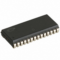
... The input/output pins remain in a high-impedance state unless the chip is selected, outputs are enabled, and Write Enable (WE) is HIGH. The CY7C1399B is available in 28-pin standard 300-mil-wide SOJ and TSOP Type I packages. I/O I/O ...
Page 2
... I CC Output Disabled V = Max GND CC OUT V = Max mA, CC OUT 1/t MAX RC Max MAX Max – 0.3V [4] V – 0.3V 0.3V – 0. 0.3V MAX CY7C1399B I GND Ambient Temperature +70 C 3.3V 300 mV – +85 C 3.3V 300 mV 7C1399B-10 7C1399B-12 Min ...
Page 3
... MAX Max –0.3V [4] V – 0.3V 0.3V –0. 0.3V, CC f=f MAX Description Test Conditions MHz 351 1.73V CY7C1399B 1399B-15 1399B-20 Min. Max. Min. Max. 2.4 2.4 0.4 0.4 2 +0.3V +0.3V –0.3 0.8 –0.3 0.8 –1 +1 –1 +1 –5 +5 –5 +5 –300 – ...
Page 4
... HIGH. The data input set-up and hold timing should be referenced to the rising edge of the signal that terminates the write. 10. The minimum write cycle time for write cycle #3 (WE controlled, OE LOW) is the sum of t Document #: 38-05071 Rev. *B [6] Description [7] [7, 8] [7] [7, 8] [9] [7] is less than less than t HZCE LZCE HZOE LZOE and t HZWE CY7C1399B 1399B-10 1399B-12 Min. Max. Min. Max ...
Page 5
... CDR Retention Time t Operation Recovery Time R Document #: 38-05071 Rev. *B [6] (Continued) Description [7] [7, 8] [7] [7, 8] [9] [7] (Over the Operating Range - L version only) Description Conditions Com’ 2.0V > V – 0.3V > V – 0. < 0.3V IN CY7C1399B 1399B-15 1399B-20 Min. Max. Min. Max ...
Page 6
... Notes: 11. Device is continuously selected HIGH for read cycle. 13. Address valid prior to or coincident with CE transition LOW. Document #: 38-05071 Rev. *B DATA RETENTION MODE 3. CDR OHA ACE t DOE t LZOE 50 CY7C1399B 3. DATA VALID t HZOE t HZCE IMPEDANCE DATA VALID t PD 50% HIGH ICC ISB Page ...
Page 7
... If CE goes HIGH simultaneously with WE HIGH, the output remains in a high-impedance state. 16. During this period, the I/Os are in the output state and input signals should not be applied. Document #: 38-05071 Rev PWE t SD DATA SCE DATA [10, 15 DATA HZWE CY7C1399B VALID VALID VALID IN t LZWE Page ...
Page 8
... H H High Z Ordering Information Speed (ns) Ordering Code 10 CY7C1399B-10VC CY7C1399B-10ZC CY7C1399BL-10VC CY7C1399BL-10ZC 12 CY7C1399B-12VC CY7C1399B-12ZC CY7C1399BL-12VC CY7C1399BL-12ZC CY7C1399B-12VI CY7C1399B-12ZI 15 CY7C1399B-15VC CY7C1399B-15ZC CY7C1399BL-15VC CY7C1399BL-15ZC CY7C1399B-15VI CY7C1399B-15ZI 20 CY7C1399B-20VC CY7C1399B-20ZC CY7C1399BL-20VC CY7C1399BL-20ZC CY7C1399B-20VI CY7C1399B-20ZI Document #: 38-05071 Rev. *B Mode Deselect/Power-Down Read Write Deselect, Output Disabled Package Name ...
Page 9
... The inclusion of Cypress Semiconductor products in life-support systems application implies that the manufacturer assumes all risk of such use and in doing so indemnifies Cypress Semiconductor against all charges. 28-Lead (300-Mil) Molded SOJ V21 CY7C1399B 51-85031-B 51-85071-*G ...
Page 10
... Document History Page Document Title: CY7C1399B 32K x 8 3.3V Static RAM Document Number: 38-05071 ISSUE REV. ECN NO. DATE ** 107264 05/25/01 *A 107533 06/28/01 *B 116472 09/17/02 Document #: 38-05071 Rev. *B ORIG. OF CHANGE DESCRIPTION OF CHANGE SZV Change from Spec #: 38-01102 to 38-05071 MAX Add Low Power CEA Add applications foot note to data sheet, page 1 ...