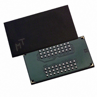
MT48H8M16LFB4-8 IT:J TR Micron Technology Inc, MT48H8M16LFB4-8 IT:J TR Datasheet - Page 53

MT48H8M16LFB4-8 IT:J TR
Manufacturer Part Number
MT48H8M16LFB4-8 IT:J TR
Description
IC SDRAM 128MBIT 125MHZ 54VFBGA
Manufacturer
Micron Technology Inc
Type
Mobile SDRAMr
Datasheet
1.MT48H8M16LFB4-8_ITJ_TR.pdf
(75 pages)
Specifications of MT48H8M16LFB4-8 IT:J TR
Format - Memory
RAM
Memory Type
Mobile SDRAM
Memory Size
128M (8Mx16)
Speed
125MHz
Interface
Parallel
Voltage - Supply
1.7 V ~ 1.9 V
Operating Temperature
-40°C ~ 85°C
Package / Case
54-VFBGA
Organization
8Mx16
Density
128Mb
Address Bus
14b
Access Time (max)
8/6ns
Maximum Clock Rate
125MHz
Operating Supply Voltage (typ)
1.8V
Package Type
VFBGA
Operating Temp Range
-40C to 85C
Operating Supply Voltage (max)
1.95V
Operating Supply Voltage (min)
1.7V
Supply Current
50mA
Pin Count
54
Mounting
Surface Mount
Operating Temperature Classification
Industrial
Lead Free Status / RoHS Status
Lead free / RoHS Compliant
Other names
557-1236-2
Figure 29:
Figure 30:
PDF: 09005aef832ff1ea/Source: 09005aef832ff1ac
sdr_mobile_sdram_cmd_op_timing_dia_fr10_08__3.fm - Rev. E 4/09 EN
Random WRITE Cycles
WRITE-to-READ
Notes:
Notes:
1. Each WRITE command can be to any bank. DQM is LOW.
1. The WRITE command can be to any bank, and the READ command can be to any bank.
Command
Command
Address
Address
DQM is LOW. CL = 2 for illustration.
CLK
CLK
DQ
DQ
WRITE
WRITE
Bank,
Col n
Bank,
Col n
Din
Din
T0
T0
n
n
WRITE
Bank,
n + 1
Col a
NOP
Din
Din
T1
T1
a
128Mb: 8 Meg x 16, 4 Meg x 32 Mobile SDRAM
53
WRITE
Bank,
Col x
READ
Bank,
Din
Col b
T2
T2
x
Don’t Care
Micron Technology, Inc., reserves the right to change products or specifications without notice.
WRITE
Col m
Bank,
T3
Din
T3
NOP
m
Dout
NOP
T4
b
Don’t Care
NOP
Dout
b + 1
T5
©2008 Micron Technology, Inc. All rights reserved.
Timing Diagrams


