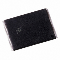
MT28F128J3RP-12 ET TR Micron Technology Inc, MT28F128J3RP-12 ET TR Datasheet - Page 15

MT28F128J3RP-12 ET TR
Manufacturer Part Number
MT28F128J3RP-12 ET TR
Description
IC FLASH 128MBIT 120NS 56TSOP
Manufacturer
Micron Technology Inc
Datasheet
1.MT28F128J3FS-12_ET_TR.pdf
(55 pages)
Specifications of MT28F128J3RP-12 ET TR
Format - Memory
FLASH
Memory Type
FLASH
Memory Size
128M (16Mx8, 8Mx16)
Speed
120ns
Interface
Parallel
Voltage - Supply
2.7 V ~ 3.6 V
Operating Temperature
-40°C ~ 85°C
Package / Case
56-TSOP
Lead Free Status / RoHS Status
Lead free / RoHS Compliant
NOTE:
10. The number of bytes/words to be written to the write buffer = n + 1, where n = byte/word count argument. Count
11. The WRITE-to-BUFFER or ERASE operation does not begin until a CONFIRM command (D0h) is issued.
12. Attempts to issue a block erase or program to a locked block will fail.
13. Either 40h or 10h is recognized by the ISM as the byte/word program setup.
14. Program suspend can be issued after either the WRITE-to-BUFFER or WORD/BYTE PROGRAM operation is initiated.
09005aef80b5a323
MT28F640J3.fm – Rev. N 3/05 EN
1. Commands other than those shown in Table 4 on page 14 are reserved for future device implementations and
2. The SCS is also referred to as the extended command set.
3. Bus operations are defined in Table 3 on page 13.
4. X
5. ID = Data read from identifier codes
6. The upper byte of the data bus (DQ8–DQ15) during command WRITEs is a “Don’t Care” in x16 operation.
7. Following the READ IDENTIFIER CODES command, READ operations access manufacturer, device, and block lock
8. If the ISM is running, only DQ7 is valid; DQ15–DQ8 and DQ6–DQ0 are placed in High-Z.
9. After the WRITE-to-BUFFER command is issued, check the XSR to make sure a buffer is available for writing.
The CLEAR BLOCK LOCK BITS operation simultaneously clears all block lock bits.
should not be used.
BA = Address within the block
IA = Identifier code address; see Figure 7 on page 12 and Table 16 on page 23
QA = Query data base address
PA = Address of memory location to be programmed
QD = Data read from query data base
SRD = Data read from status register; see Table 17 on page 24 for a description of the status register bits
PD = Data to be programmed at location PA; data is latched on the rising edge of WE#
CC = Configuration code
codes. See Block Status Register section for read identifier code data.
ranges on this device for byte mode are n = 00h to n = 1Fh and for word mode, n = 0000h to n = 000Fh. The third
and consecutive bus cycles, as determined by n, are for writing data into the write buffer. The CONFIRM command
(D0h) is expected after exactly n + 1 WRITE cycles; any other command at that point in the sequence aborts the
WRITE-to-BUFFER operation. Please see Figure 9 on page 31, WRITE-to-BUFFER Flowchart, for additional informa-
tion.
= Any valid address within the device
15
Micron Technology, Inc., reserves the right to change products or specifications without notice.
128Mb, 64Mb, 32Mb
Q-FLASH MEMORY
©2000 Micron Technology. Inc.


