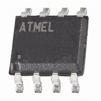
AT45DB081D-SU Atmel, AT45DB081D-SU Datasheet - Page 18

AT45DB081D-SU
Manufacturer Part Number
AT45DB081D-SU
Description
IC FLASH 8MBIT 66MHZ 8SOIC
Manufacturer
Atmel
Specifications of AT45DB081D-SU
Format - Memory
FLASH
Memory Type
DataFLASH
Memory Size
8M (4096 pages x 264 bytes)
Speed
66MHz
Interface
SPI, RapidS
Voltage - Supply
2.7 V ~ 3.6 V
Operating Temperature
-40°C ~ 85°C
Package / Case
8-SOIC (5.3mm Width), 8-SOP, 8-SOEIAJ
Architecture
Sectored
Interface Type
SPI
Supply Voltage (max)
3.6 V
Supply Voltage (min)
2.7 V
Maximum Operating Current
15 mA
Mounting Style
SMD/SMT
Organization
64 KB x 16
Memory Configuration
4096 Pages X 264 Bytes
Clock Frequency
50MHz
Supply Voltage Range
2.5V To 3.6V, 2.7V To 3.6V
Rohs Compliant
Yes
Lead Free Status / RoHS Status
Lead free / RoHS Compliant
Available stocks
Company
Part Number
Manufacturer
Quantity
Price
Company:
Part Number:
AT45DB081D-SU
Manufacturer:
ATMEL
Quantity:
750
Company:
Part Number:
AT45DB081D-SU
Manufacturer:
ATMEL
Quantity:
8
Part Number:
AT45DB081D-SU
Manufacturer:
ATMEL/爱特梅尔
Quantity:
20 000
Part Number:
AT45DB081D-SU-2.5
Manufacturer:
ATMEL/爱特梅尔
Quantity:
20 000
10.1.1
10.1.2
Figure 10-2. Read Sector Lockdown Register
18
CS
SO
Atmel AT45DB081D
Sector Lockdown Register
Reading the Sector Lockdown Register
SI
Each transition
represents 8 bits
Opcode
Sector Lockdown Register is a nonvolatile register that contains 16-bytes of data, as shown
below:
Table 10-2.
Table 10-3.
The Sector Lockdown Register can be read to determine which sectors in the memory array are
permanently locked down. To read the Sector Lockdown Register, the CS pin must first be
asserted. Once the CS pin has been asserted, an opcode of 35H and three dummy bytes must
be clocked into the device via the SI pin. After the last bit of the opcode and dummy bytes have
been clocked in, the data for the contents of the Sector Lockdown Register will be clocked out
on the SO pin. The first byte corresponds to sector 0 (0a, 0b) the second byte corresponds to
sector one and the las byte (byte 16) corresponds to sector 15. After the last byte of the Sector
Lockdown Register has been read, additional pulses on the SCK pin will simply result in unde-
fined data being output on the SO pin.
Deasserting the CS pin will terminate the Read Sector Lockdown Register operation and put the
SO pin into a high-impedance state.
Table 10-4
Table 10-4.
Sector Number
Locked
Unlocked
Sectors 0a, 0b Unlocked
Sector 0a Locked (Page 0-7)
Sector 0b Locked (Page 8-255)
Sectors 0a, 0b Locked (Page 0-255)
Command
Read Sector Lockdown Register
Note:
xx = Dummy Byte
details the values read from the Sector Lockdown Register.
X
Sector Lockdown Register
Sector 0 (0a, 0b)
Sector Lockdown Register
X
X
(Page 0-7)
Bit 7, 6
Data Byte
0a
00
11
00
11
n
Byte 1
35H
See Below
0 (0a, 0b)
(Page 8-255)
Data Byte
Bit 5, 4
n + 1
0b
00
00
11
11
Byte 2
xxH
Bit 3, 2
00
00
00
00
Data Byte
Byte 3
n + 15
xxH
Bit 1, 0
1 to 15
00
00
00
00
3596M–DFLASH–5/10
FFH
00H
Byte 4
xxH
Value
Data
C0H
F0H
00H
30H


