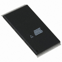
AT49BV163AT-70TI Atmel, AT49BV163AT-70TI Datasheet - Page 7

AT49BV163AT-70TI
Manufacturer Part Number
AT49BV163AT-70TI
Description
IC FLASH 16MBIT 70NS 48TSOP
Manufacturer
Atmel
Datasheet
1.AT49BV163AT-70TI.pdf
(29 pages)
Specifications of AT49BV163AT-70TI
Format - Memory
FLASH
Memory Type
FLASH
Memory Size
16M (2M x 8 or 1M x 16)
Speed
70ns
Interface
Parallel
Voltage - Supply
2.65 V ~ 3.6 V
Operating Temperature
-40°C ~ 85°C
Package / Case
48-TSOP
Lead Free Status / RoHS Status
Contains lead / RoHS non-compliant
Available stocks
Company
Part Number
Manufacturer
Quantity
Price
Company:
Part Number:
AT49BV163AT-70TI
Manufacturer:
ATMEL
Quantity:
680
Company:
Part Number:
AT49BV163AT-70TI
Manufacturer:
ATMEL
Quantity:
1 844
AT49BV162/163A(T)
SECTOR LOCKDOWN OVERRIDE: The only way to unlock a sector that is locked down is
through reset or power-up cycles. After power-up or reset, the content of a sector that is
locked down can be erased and reprogrammed.
ERASE SUSPEND/ERASE RESUME: The Erase Suspend command allows the system to
interrupt a sector or chip erase operation and then program or read data from a different sector
within the memory. After the Erase Suspend command is given, the device requires a maxi-
mum time of 15 µs to suspend the erase operation. After the erase operation has been
suspended, the system can then read data or program data to any other sector within the
device. An address is not required during the Erase Suspend command. During a sector erase
suspend, another sector cannot be erased. To resume the sector erase operation, the system
must write the Erase Resume command. The Erase Resume command is a one-bus cycle
command. The device also supports an erase suspend during a complete chip erase. While
the chip erase is suspended, the user can read from any sector within the memory that is pro-
tected. The command sequence for a chip erase suspend and a sector erase suspend are the
same.
PROGRAM SUSPEND/PROGRAM RESUME: The Program Suspend command allows the
system to interrupt a programming operation and then read data from a different byte/word
within the memory. After the Program Suspend command is given, the device requires a max-
imum of 20 µs to suspend the programming operation. After the programming operation has
been suspended, the system can then read data from any other byte/word that is not con-
tained in the sector in which the programming operation was suspended. An address is not
required during the program suspend operation. To resume the programming operation, the
system must write the Program Resume command. The program suspend and resume are
one-bus cycle commands. The command sequence for the erase suspend and program sus-
pend are the same, and the command sequence for the erase resume and program resume
are the same.
PRODUCT IDENTIFICATION: The product identification mode identifies the device and man-
ufacturer as Atmel. It is accessed using a software operation.
For details, see “Operating Modes” on page 16 or “Software Product Identification Entry/Exit”
sections on page 23.
128-BIT PROTECTION REGISTER: The AT49BV162A(T)/163A(T) contains a 128-bit register
that can be used for security purposes in system design. The protection register is divided into
two 64-bit blocks. The two blocks are designated as block A and block B. The data in block A
is non-changeable and is programmed at the factory with a unique number. The data in block
B is programmed by the user and can be locked out such that data in the block cannot be
reprogrammed. To program block B in the protection register, the four-bus cycle Program Pro-
tection Register command must be used as shown in the “Command Definition in Hex” table
on page 12. To lock out block B, the four-bus cycle Lock Protection Register command must
be used as shown in the “Command Definition in Hex” table. Data bit D1 must be zero during
the fourth bus cycle. All other data bits during the fourth bus cycle are don’t cares. To deter-
mine whether block B is locked out, the Product ID Entry command is given followed by a read
operation from address 80H. If data bit D1 is zero, block B is locked. If data bit D1 is one, block
B can be reprogrammed. Please see the “Protection Register Addressing Table” on page 13
for the address locations in the protection register. To read the protection register, the Product
ID Entry command is given followed by a normal read operation from an address within the
protection register. After determining whether block B is protected or not, or reading the pro-
tection register, the Product ID Exit command must be given prior to performing any other
operation.
RDY/BUSY: An open-drain READY/BUSY output pin provides another method of detecting
the end of a program or erase operation. RDY/BUSY is actively pulled low during the internal
program and erase cycles and is released at the completion of the cycle. The open-drain con-
7
3349G–FLASH–7/04


