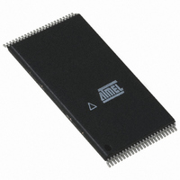
AT49BV163AT-70TI Atmel, AT49BV163AT-70TI Datasheet - Page 5

AT49BV163AT-70TI
Manufacturer Part Number
AT49BV163AT-70TI
Description
IC FLASH 16MBIT 70NS 48TSOP
Manufacturer
Atmel
Datasheet
1.AT49BV163AT-70TI.pdf
(29 pages)
Specifications of AT49BV163AT-70TI
Format - Memory
FLASH
Memory Type
FLASH
Memory Size
16M (2M x 8 or 1M x 16)
Speed
70ns
Interface
Parallel
Voltage - Supply
2.65 V ~ 3.6 V
Operating Temperature
-40°C ~ 85°C
Package / Case
48-TSOP
Lead Free Status / RoHS Status
Contains lead / RoHS non-compliant
Available stocks
Company
Part Number
Manufacturer
Quantity
Price
Company:
Part Number:
AT49BV163AT-70TI
Manufacturer:
ATMEL
Quantity:
680
Company:
Part Number:
AT49BV163AT-70TI
Manufacturer:
ATMEL
Quantity:
1 844
AT49BV162/163A(T)
Any commands written to the chip during the embedded programming cycle will be ignored. If
a hardware reset happens during programming, the data at the location being programmed
will be corrupted. Please note that a data “0” cannot be programmed back to a “1”; only erase
operations can convert “0”s to “1”s. Programming is completed after the specified t
cycle
BP
time. The Data Polling feature or the Toggle Bit feature may be used to indicate the end of a
program cycle. If the erase/program status bit is a “1”, the device was not able to verify that the
erase or program operation was performed successfully.
VPP PIN: The circuitry of the AT49BV162A(T) is designed so that the device cannot be pro-
grammed or erased if the V
voltage is less that 0.4V. When V
is at 0.9V or above, normal
PP
PP
program and erase operations can be performed. The VPP pin cannot be left floating.
PROGRAM/ERASE STATUS: The device provides several bits to determine the status of a
program or erase operation: I/O2, I/O3, I/O5, I/O6 and I/O7. The “Status Bit Table” on page 11
and the following four sections describe the function of these bits. To provide greater flexibility
for system designers, the AT49BV162A(T)/163A(T) contains a programmable configuration
register. The configuration register allows the user to specify the status bit operation. The con-
figuration register can be set to one of two different values, “00” or “01”. If the configuration
register is set to “00”, the part will automatically return to the read mode after a successful pro-
gram or erase operation. If the configuration register is set to a “01”, a Product ID Exit
command must be given after a successful program or erase operation before the part will
return to the read mode. It is important to note that whether the configuration register is set to
a “00” or to a “01”, any unsuccessful program or erase operation requires using the Product ID
Exit command to return the device to read mode. The default value (after power-up) for the
configuration register is “00”. Using the four-bus cycle Set Configuration Register command as
shown in the “Command Definition in Hex” table on page 12, the value of the configuration
register can be changed. Voltages applied to the RESET pin will not alter the value of the con-
figuration register. The value of the configuration register will affect the operation of the I/O7
status bit as described below.
DATA POLLING: The AT49BV162A(T)/163A(T) features Data Polling to indicate the end of a
program cycle. If the status configuration register is set to a “00”, during a program cycle an
attempted read of the last byte/word loaded will result in the complement of the loaded data on
I/O7. Once the program cycle has been completed, true data is valid on all outputs and the
next cycle may begin. During a chip or sector erase operation, an attempt to read the device
will give a “0” on I/O7. Once the program or erase cycle has completed, true data will be read
from the device. Data Polling may begin at any time during the program cycle. Please see
“Status Bit Table” on page 11 for more details.
If the status bit configuration register is set to a “01”, the I/O7 status bit will be low while the
device is actively programming or erasing data. I/O7 will go high when the device has com-
pleted a program or erase operation. Once I/O7 has gone high, status information on the other
pins can be checked.
The Data Polling status bit must be used in conjunction with the erase/program and V
status
PP
bit as shown in the algorithm in Figures 1 and 2 on page 9.
5
3349G–FLASH–7/04


